
Methods of Forming Dual-Damascene Metal Wiring Patterns for Integrated Circuit Devices and Wiring Patterns Formed Thereby

a technology of metal wiring pattern and integrated circuit device, which is applied in the direction of semiconductor device, semiconductor/solid-state device details, electrical apparatus, etc., can solve the problems of affecting the reliability of the device, preventing the formation of a uniform first, and leaking curren

Active Publication Date: 2007-02-08
SAMSUNG ELECTRONICS CO LTD
View PDF4 Cites 34 Cited by
  • Summary
  • Abstract
  • Description
  • Claims
  • Application Information

AI Technical Summary

Problems solved by technology

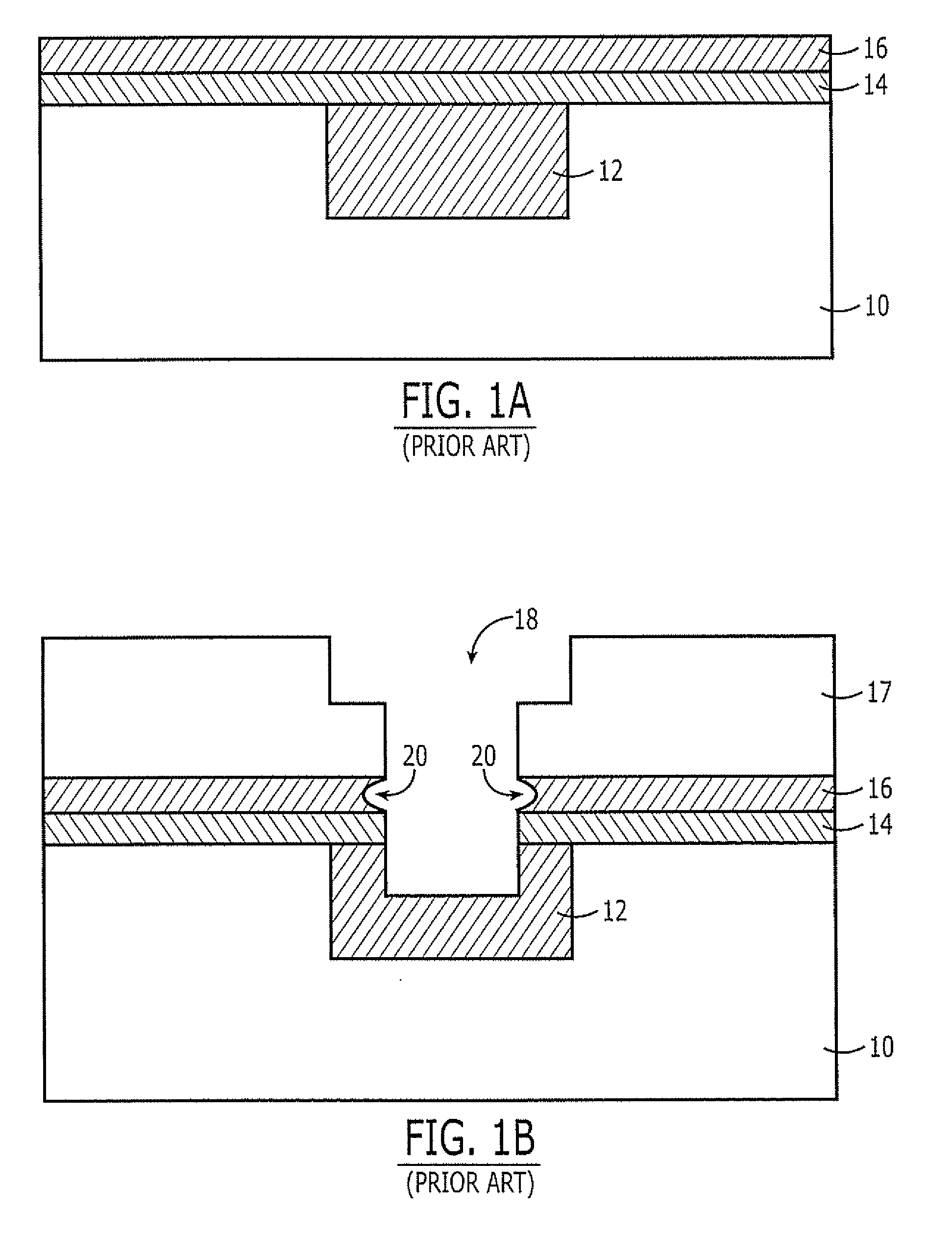
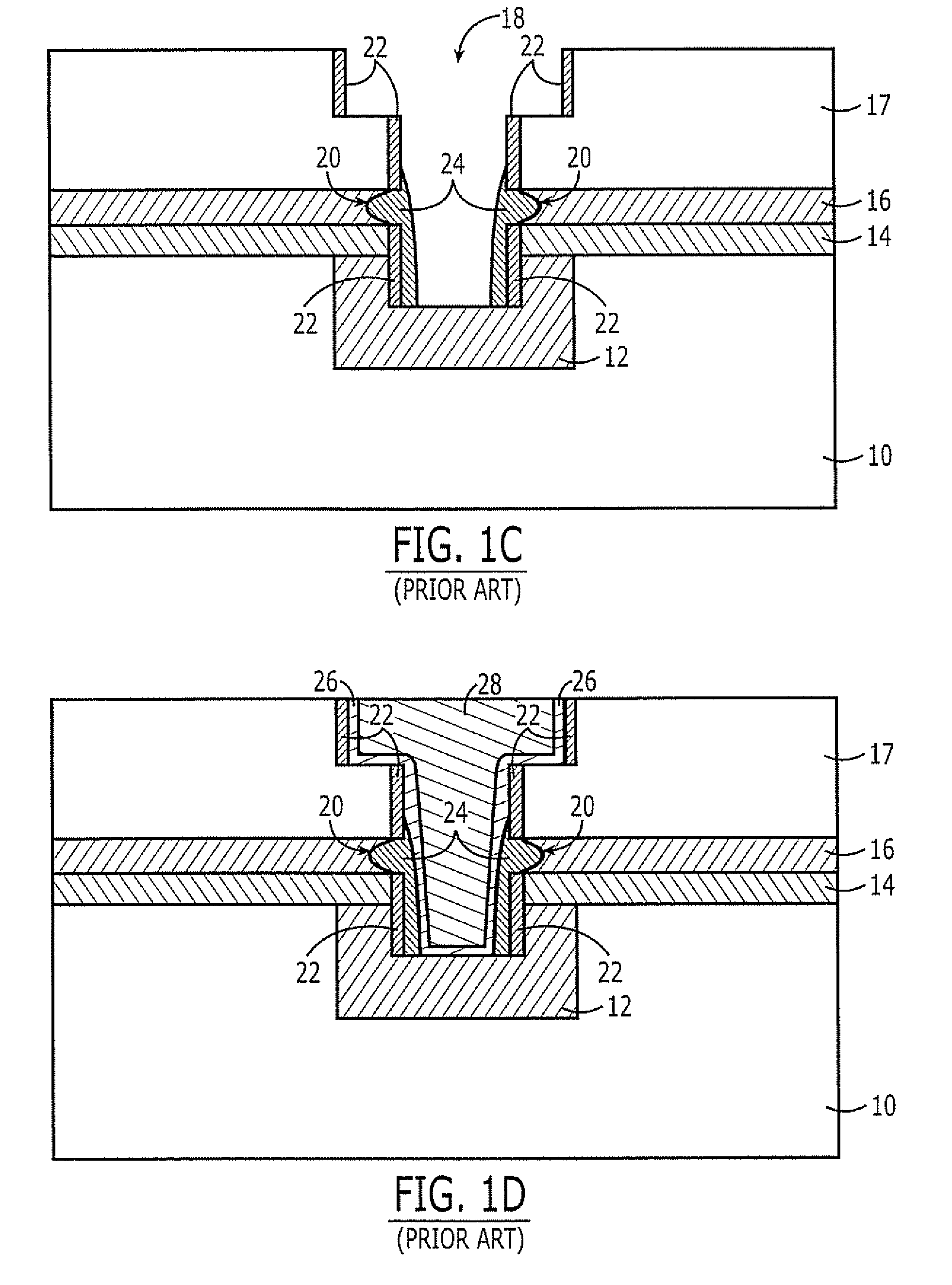
However, this exposure to the wet cleaning solution may also result in the formation of undercut regions 20 within the electrically insulating layer 16, which may react with the cleaning solution.
Unfortunately, the presence of the undercut regions 20 may preclude the formation of a uniform first barrier metal layer on the sidewall of the via hole 18.
This increase in leakage current may degrade device reliability by increasing time dependent dielectric breakdown (TDDB) within the second low-K dielectric layer 17.

Method used


Image

  • Methods of Forming Dual-Damascene Metal Wiring Patterns for Integrated Circuit Devices and Wiring Patterns Formed Thereby
  • Methods of Forming Dual-Damascene Metal Wiring Patterns for Integrated Circuit Devices and Wiring Patterns Formed Thereby
  • Methods of Forming Dual-Damascene Metal Wiring Patterns for Integrated Circuit Devices and Wiring Patterns Formed Thereby

Examples


Embodiment Construction

[0015] The present invention now will be described more fully herein with reference to the accompanying drawings, in which preferred embodiments of the invention are shown. This invention may, however, be embodied in many different forms and should not be construed as being limited to the embodiments set forth herein; rather, these embodiments are provided so that this disclosure will be thorough and complete, and will fully convey the scope of the invention to those skilled in the art. Like reference numerals refer to like elements throughout.

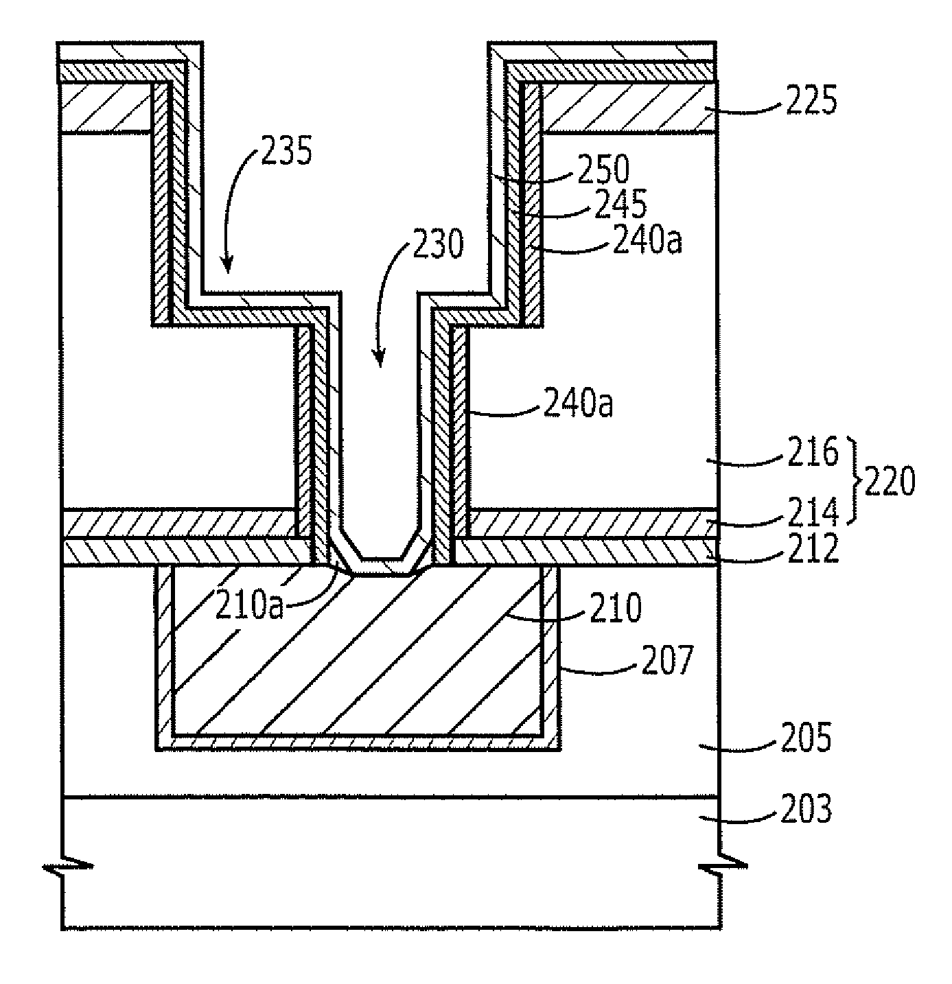
[0016] Methods of forming dual-damascene copper interconnect structures according to embodiments of the present invention include forming a first dielectric layer 205 on a primary surface of a semiconductor substrate 203 having a plurality of active semiconductor devices (not shown) therein. This first dielectric layer 205 may be a low-K dielectric layer, such as SiCOH, having a thickness in a range from about 2,000 Å to about 20,000 Å. There...


PUM


Abstract

Methods of forming dual-damascene metal wiring patterns include forming a first metal wiring pattern (e.g., copper wiring pattern) on an integrated circuit substrate and forming an etch-stop layer on the first metal wiring pattern. These steps are followed by the steps of forming an electrically insulating layer on the etch-stop layer and forming an inter-metal dielectric layer on the electrically insulating layer. The inter-metal dielectric layer and the electrically insulating layer are selectively etched in sequence to define an opening therein that exposes a first portion of the etch-stop layer. This opening may include a trench and a via hole extending downward from a bottom of the trench. A first barrier metal layer is formed on a sidewall of the opening and directly on the first portion of the etch-stop layer. A portion of the first barrier metal layer is selectively removed from the first portion of the etch-stop layer. The first portion of the etch-stop layer is then selectively etched for a sufficient duration to expose a portion of the first metal wiring pattern. A second metal wiring pattern is formed in the opening in order to complete a dual-damascene structure.

Description

REFERENCE TO PRIORITY APPLICATION [0001] This application claims priority to Korean Patent Application No. 2005-72006, filed Aug. 6, 2005, the disclosure of which is hereby incorporated herein by reference. FIELD OF THE INVENTION [0002] The present invention relates to methods of forming metal wiring patterns and, more particularly, to methods of forming metal wiring patterns using dual-damascene techniques and metal wiring patterns formed thereby. BACKGROUND OF THE INVENTION [0003] Metal wiring patterns used in integrated circuit devices are frequently formed of copper (Cu) because copper has a relatively low resistivity, particularly compared to metal wiring patterns formed of other materials such as aluminum (Al). These metal wiring patterns are frequently separated from each other by intermetal dielectric layers. In order to reduce the parasitic capacitance between adjacent metal wiring patterns and reduce their RC delay, dielectric layers having relatively low dielectric consta...

Claims


Application Information

Patent Timeline
IPC IPC(8): H01L21/44
CPCH01L21/76805H01L21/76807H01L21/76832H01L21/76834H01L21/76844H01L2924/0002H01L21/76846H01L2924/00H01L21/28
Inventor LEE, BOUNG JUSHIN, HEON JONGKANG, HEE SUNG
Owner SAMSUNG ELECTRONICS CO LTD
Learn More