

Method of making stacked die package
a technology of stacked die and package, which is applied in the field of making stacked die package, can solve the problems of inflexibility in the sequence in which the dice are stacked, the most known method of forming stacked flip chip package is complicated and costly,
- Summary
- Abstract
- Description
- Claims
- Application Information
AI Technical Summary
Benefits of technology
Problems solved by technology
Method used
Image

Examples
Embodiment Construction
[0015] The detailed description set forth below in connection with the appended drawings is intended as a description of the presently preferred embodiments of the invention, and is not intended to represent the only forms in which the present invention may be practiced. It is to be understood that the same or equivalent functions may be accomplished by different embodiments that are intended to be encompassed within the spirit and scope of the invention. In the drawings, like numerals are used to indicate like elements throughout.
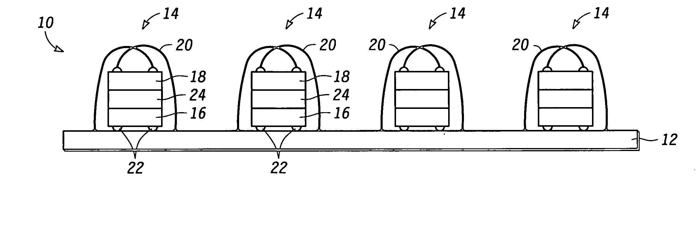
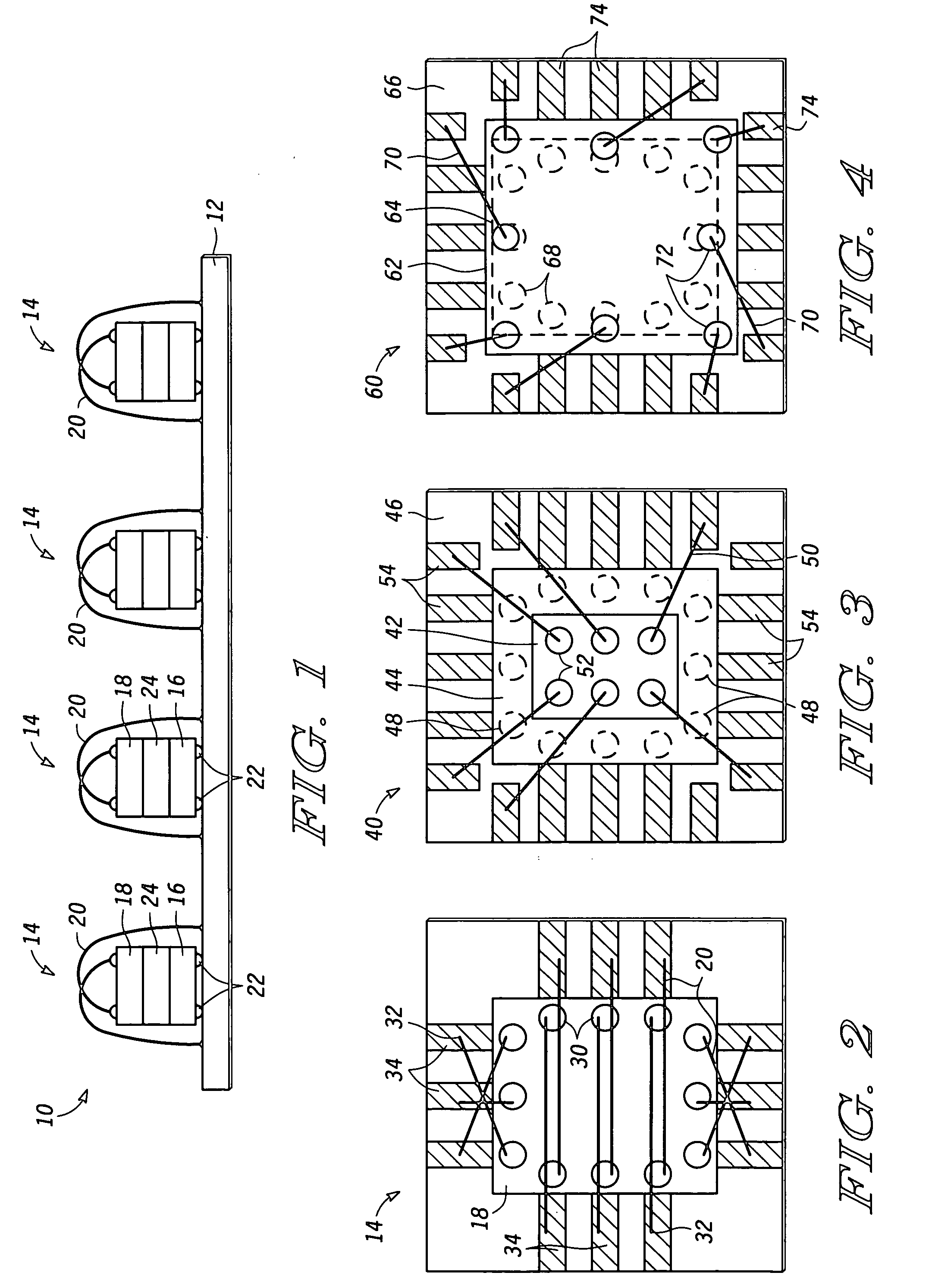
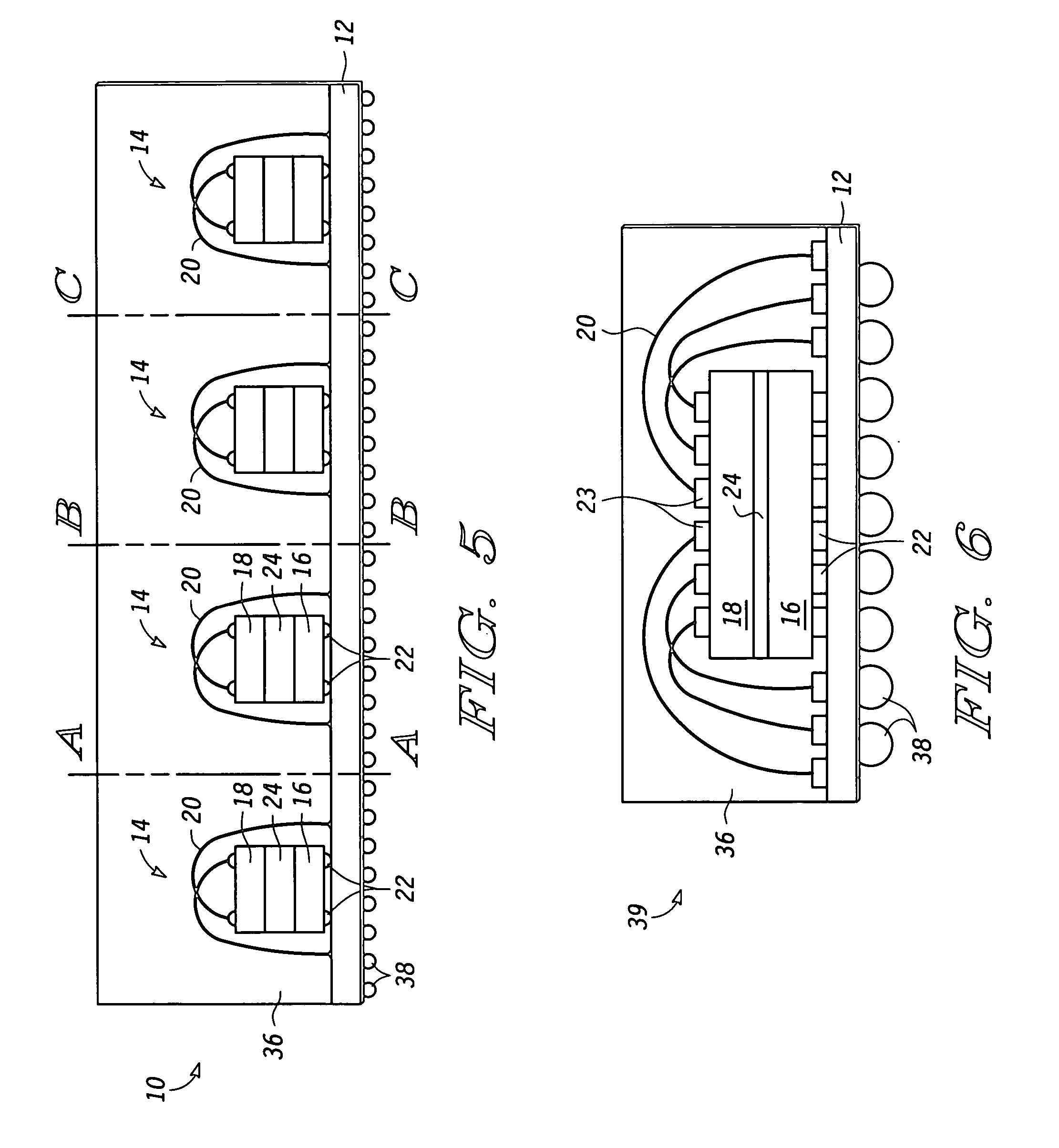
[0016] The present invention provides a method of making a stacked die package including the steps of placing a first flip chip die on a base carrier and electrically connecting the first flip chip die to the base carrier. A second flip chip die is attached back-to-back to the first flip chip die and is electrically connected to the base carrier with a plurality of insulated wires.
[0017] The present invention also provides a method of making a stacked di...
PUM
 Abstract
Description
Claims
Application Information