Trench insulation structures and methods

a technology of trench insulation and trench walls, applied in the direction of basic electric elements, semiconductor/solid-state device manufacturing, electric apparatus, etc., can solve the problems of trench walls being damaged, wet etch rate gradients, poor rebonding, etc., to improve the density of a spin-on dielectric

Active Publication Date: 2007-05-17
MICRON TECH INC
View PDF26 Cites 339 Cited by
  • Summary
  • Abstract
  • Description
  • Claims
  • Application Information

AI Technical Summary

Problems solved by technology

Integrated circuit (IC) manufacturers increasingly face difficulties with scaling and insulation between components with ever decreasing feature sizes.
During the deposition process and subsequent steps, however, the trench walls can be damaged.
However, the use of SOD insulators in the trench can also raise issues upon the conversion from liquid precursor to its final insulating form.
Three interrelated problems arise upon the conversion from precursor to insulation material: poor rebonding, volume shrinkage, and wet etch rate gradients.
These bonds and the general crystal structure can be weakened due to the volume shrinkage during densification of the SOD material pulling the SOD material away from the sidewalls.
This can change the angles in the crystal structure, resulting in easily broken bonds and high etch rates.
If the trench fill material has different etch rates in different regions, it will be hard to control the etch processes to avoid removing the trench fill.
This problem is particularly true at the walls of the trench, where the fill material is less dense due to volume shrinkage.
The etch process can create voids along the walls of the trench, reducing the effectiveness of the trench structure as an isolating device.
Problems relating to the formation of the densified SOD material are common and can cause significant problems for IC designers.

Method used


Image

  • Trench insulation structures and methods
  • Trench insulation structures and methods
  • Trench insulation structures and methods

Examples


Embodiment Construction

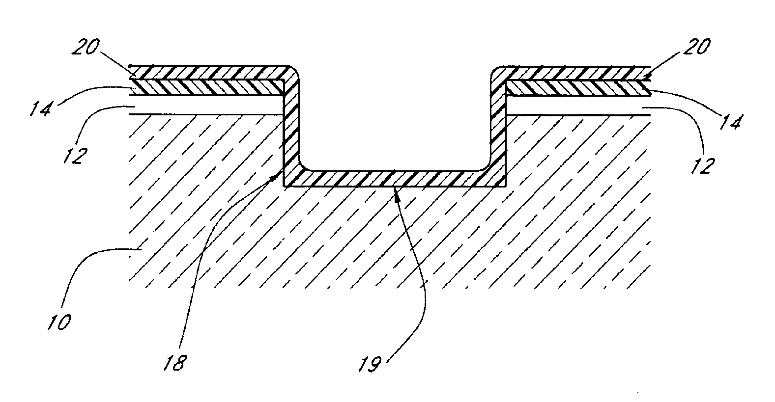
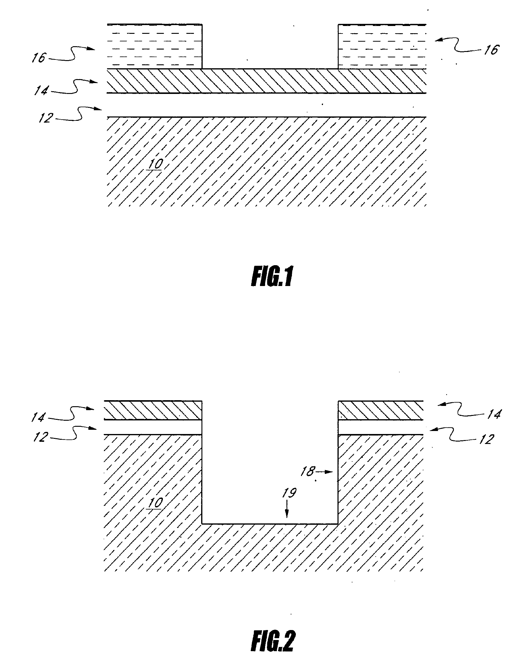
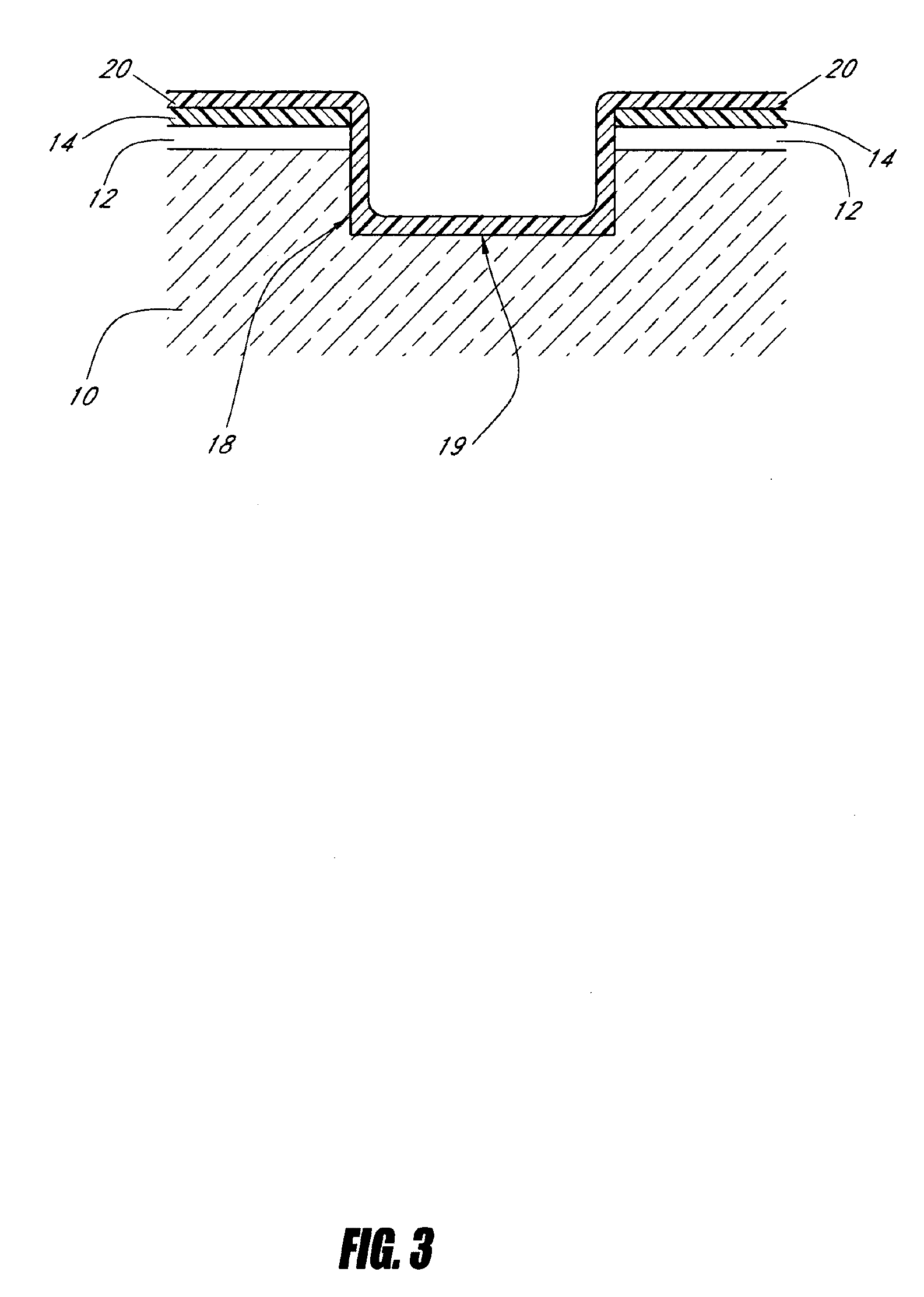
[0025] It has been found that the undesirable etch rate gradients can be attributed to the volume shrinkage of insulation materials in trenches and the associated weak crystal structure. Normal shrinkage of spin-on deposition (SOD) dielectric materials is believed to cause increased tensile bond stress and a weakened interface between densified SOD dielectrics and trench walls.

[0026] Thus, the inventors have found it desirable to anisotropically treat the base of the trench. In one embodiment, a silicon rich base layer is deposited over the base of the trench. In another embodiment, an insulating liner layer is treated using an anisotropic plasma process which produces a thin silicon rich portion of the liner layer. In either of the above embodiments, the silicon rich layer will expand upon densification of the spin-on deposition material and at least partially compensate for the volume shrinkage of the SOD material.

[0027] In a preferred embodiment, described in more detail below,...


PUM

PropertyMeasurementUnit
poweraaaaaaaaaa
poweraaaaaaaaaa
poweraaaaaaaaaa

Abstract

A method of depositing dielectric material into sub-micron spaces and resultant structures is provided. After a trench is etched in the surface of a wafer, a liner layer preferably is deposited into the trench. An anisotropic plasma process is then performed on the trench. A silicon layer may be deposited on the base of the trench during the plasma process, or the plasma can treat the liner layer. The trench is then filled with a spin-on precursor. A densification or reaction process is then applied to convert the spin-on material into an insulator, and oxidizing the silicon rich layer on the base of the trench. The resulting trench has a consistent etch rate from top to bottom of the trench.

Description

CROSS-REFERENCE TO RELATED APPLICATIONS [0001] This application is a divisional of U.S. patent application Ser. No. 11 / 009,665, filed Dec. 10, 2004, which is incorporated herein by reference.FIELD OF THE INVENTION [0002] This invention relates generally to the field of integrated circuit fabrication, and more specifically to trench isolation and methods therefor. BACKGROUND OF THE INVENTION [0003] Integrated circuit (IC) manufacturers increasingly face difficulties with scaling and insulation between components with ever decreasing feature sizes. Even though packing transistors closer is important to the concept of increasing IC speed and decreasing size, they must still be electrically separated from each other. One method of keeping transistors separate from each other is known as trench isolation. Trench isolation is the practice of creating trenches in the substrate in order to separate electrical components on the chip. The trenches are typically filled with an insulator that w...

Claims


Application Information

Patent Timeline
Patent Type & Authority Applications(United States)
IPC IPC(8): H01L21/76
CPCH01L21/76224
Inventor SMYTHE, JOHN A. IIIBUDGE, WILLIAM
Owner MICRON TECH INC
Why Eureka
Try Eureka