Flash Heating in Atomic Layer Deposition

a technology of atomic layer and flash heating, which is applied in the direction of electric heating, electric/magnetic/electromagnetic heating, coating, etc., can solve the problems of contaminant introduction into the deposited film, poor and not going to completion, so as to reduce the incorporation and reduce the incorporation of impurities , the effect of improving the quality of the deposited film

Inactive Publication Date: 2007-12-06
SANDISK TECH LLC
View PDF68 Cites 337 Cited by
  • Summary
  • Abstract
  • Description
  • Claims
  • Application Information

AI Technical Summary

Benefits of technology

[0153]It should be noted that in flash memory chips, the convention has been to use the same floating gate oxide that is used between the floating gate and the channel for the gate oxide of low, and some medium voltage transistors in order to save extra process steps. Therefore the conventional tunnel oxide with a thickness that is usually greater than 8 nm has been limiting the performance, sub-threshold slope, and on-current drive of the low and some medium voltage transistors. This has resulted in slower program, and read characteristics. One advantage of the present invention is to provide a peripheral transistor gate oxide that is electrically and effectively much thinner than the conventional tunnel oxide, and is physically thicker than the conventional tunnel oxide. In other words, the peripheral circuitry will benefit from replacing the conventional tunnel oxide gate with high-K material(s) in alignment with the general trend of the semiconductor industry towards high-K materials.
[0154]Step 1202 of FIG. 25 includes performing implants and associated anneals of the triple well. The result of step 1202 is depicted in FIG. 26A, which depicts P substrate 1018, N-well 1022 within P-substrate 1018, and P-Well 1020 within N-well 1022. The sidewalls of the N-well that isolate the P-wells from one another are not depicted. Also the N-well depth is typically much thicker than that of the P-well in contrast to FIG. 26A. The P substrate is usually the thickest consisting of the majority of the wafer thickness. In step 1204, the high-K material(s) is deposited on top of P-Well 1020. The high-K material may be deposited using Atomic Layer Deposition (ALD) in accordance with various embodiments as described herein. Additionally (and optionally), other materials may be deposited on, deposited under or incorporated within the high-K material in order to form dielectric layer 1030. The result of step 1204 is depicted in FIG. 26B, which shows dielectric layer 1030, with the high-K material. Note that one advantage of using the high-K material in the lower dielectric layer is that it can also be used for low voltage peripheral transistors to increase performance.
[0155]In accordance with one embodiment, step 1204 can include the deposition of a high-K material using one or more of the techniques as preiously described. For example, a high-density plasma deposition system can be used that utilizes a Kr feed gas in combination with a plasma chamber bias, wafer bias, selectively permeable membrane, and / or additional particle dissociating energy source to deposit an oxide, nitride, oxynitride or other suitable high-K material. In one embodiment, the high-K material can be flash heated after one or more deposition cycles to release contaminant incorporation in the substrate. As previously described, the effective thickness of the dielectric region between the channel and the floating gate should be reduced in order to maintain control of the floating gate over the channel. An ALD process incorporating Kr as an ion generating feed gas to provide high radical concentrations facilitates the deposition of a high quality dielectric having a high dielectric constant. The low thermal ALD process will minimize the diffusion of dopants, stop the poly-crystallization of the dielectric material, and minimize the inter-diffusion of silicon atoms into the material.
[0156]In accordance with various embodiments, the deposition of a high-K material at step 1204 can include the simultaneous growth of one or more interfacial layers using a high radical concentration. Interfacial layers are undesirable in typical applications, as previously discussed, given that their dielectric constant tends to be substantially lower than the dielectric constant of the high-K material. In accordance with various embodiments of the present invention, however, these interfacial layers can be beneficial, and hence, a high radical concentration is achieved to facilitate the growth of lower dielectric constant interfacial layers while performing a deposition process. While a grown interfacial layer such as SiO2 may have a lower dielectric constant, it also has a higher energy barrier (ΔEc), that reduces the possibility of electron injection into the high-K dielectric by both direct tunneling and Fowler-Nordheim tunneling. Because a storage element in accordance with embodiments is programmed by transferring a charge from the control gate across the inter poly dielectric to the floating gate, a barrier to tunneling from the channel is very beneficial. This is in contrast to typical storage elements where tunneling across the dielectric layer separating the channel from the floating gate is achieved to program and erase the cell.
[0157]A high-density plasma source chamber utilizing one or more techniques as previously described can be used in one embodiment to increase the radical concentration delivered to the reacting surface for deposition. Some of the highly reactive radicals (e.g., oxygen) can penetrate the high-K dielectric being deposited and react with the underlying silicon substrate to grow one or more interfacial layers. These interfacial layers are grown in addition to the material being deposited. For example, an Al2O3 high-K material may be deposited while one or more lower-K SiO2 interfacial layers are grown from the silicon based substrate. After the Al containing first precursor is introduced, adsorbed, and purged from the deposition chamber, oxygen radicals can be generated from a high-density plasma source and introduced to the deposition chamber, along with Kr ions, to react at the substrate surface and form a monolayer of Al2O3. Some of the oxygen radicals will reach the silicon substrate and cause the growth of SiO2.
[0158]The aforementioned simultaneous growth and deposition technique can be used when depositing any film where it is desired o produce such interfacial layers. The technique need not be practiced in conjunction with the storage cell presented herein.

Problems solved by technology

Thus, the precursors (typically gases or liquids and sometimes solids) do not mix in the gas phase such that reactions are limited to the substrate surface.
Lower temperatures, however, can also lead to poorer quality of deposited films because of the incorporation of impurities (e.g., those left over from the incomplete reaction of precursors) into the film.
If the process temperature is not accurately selected or maintained, surface reactions may not go to completion, leaving un-reacted precursor and / or byproducts on and in the deposited film.
Other factors may also lead to the contaminant introduction into a deposited film.
Typical annealing techniques to reduce impurity incorporation in films involve the heating of the bulk of the substrate and may not be suitable for industrial ALD applications.
In a low-temperature ALD process, raising the bulk temperature can introduce a delay into the ALD process while waiting for the substrate to cool back to the ALD processing temperature after annealing.
If the process is continued at a high temperature, gas-phase precursor reactions, agglomeration, and other negative effects can occur.

Method used


Image

  • Flash Heating in Atomic Layer Deposition
  • Flash Heating in Atomic Layer Deposition
  • Flash Heating in Atomic Layer Deposition

Examples


Embodiment Construction

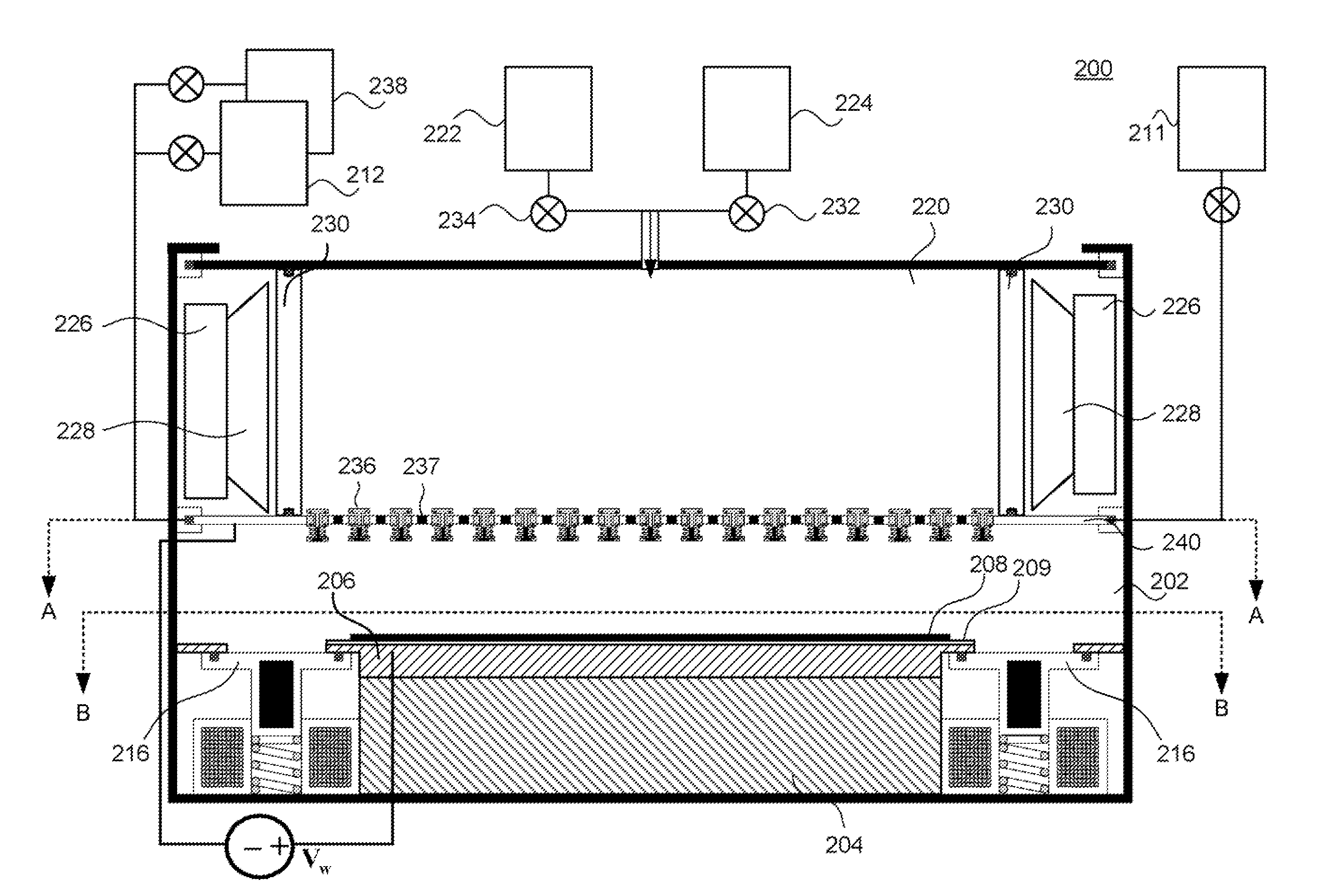
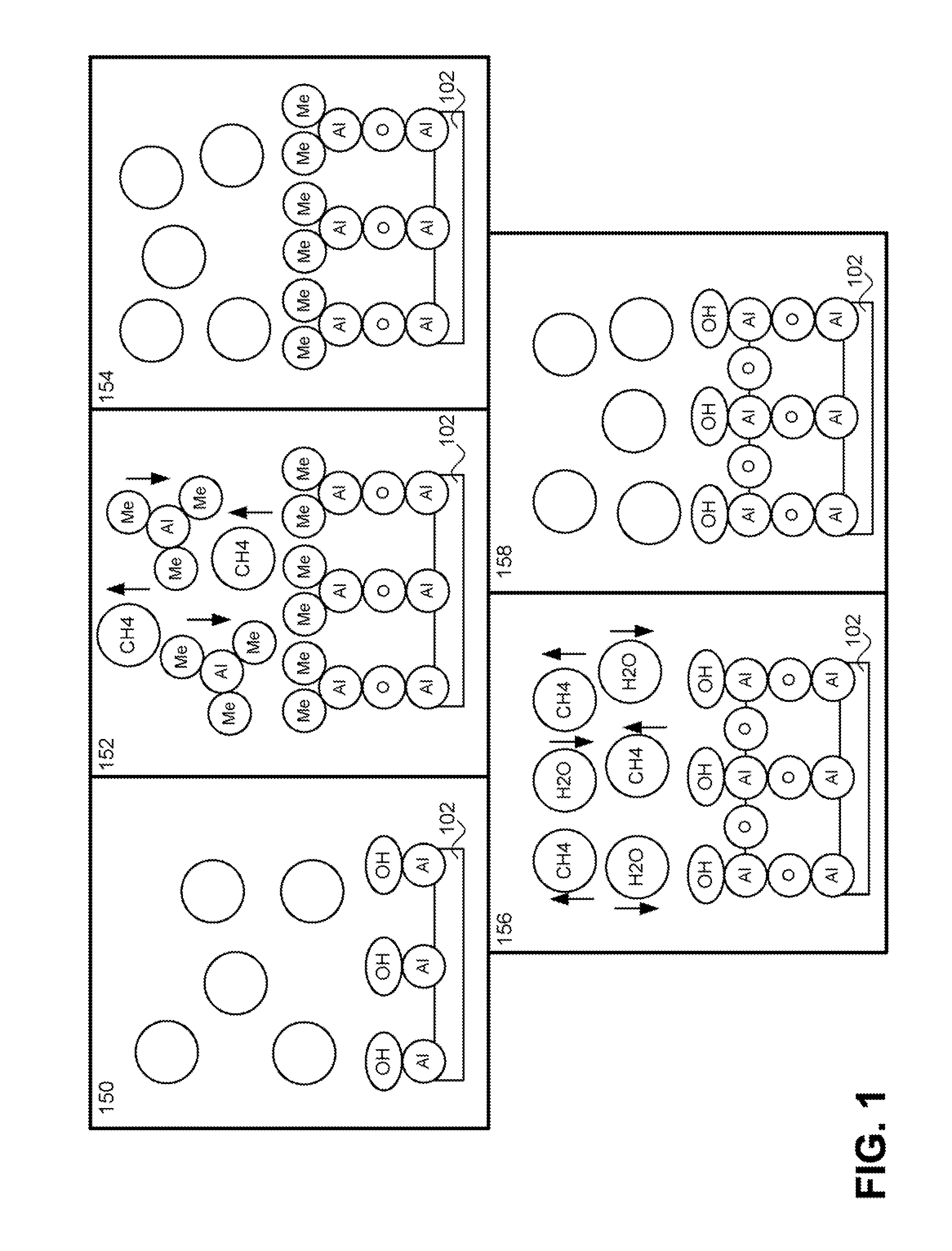
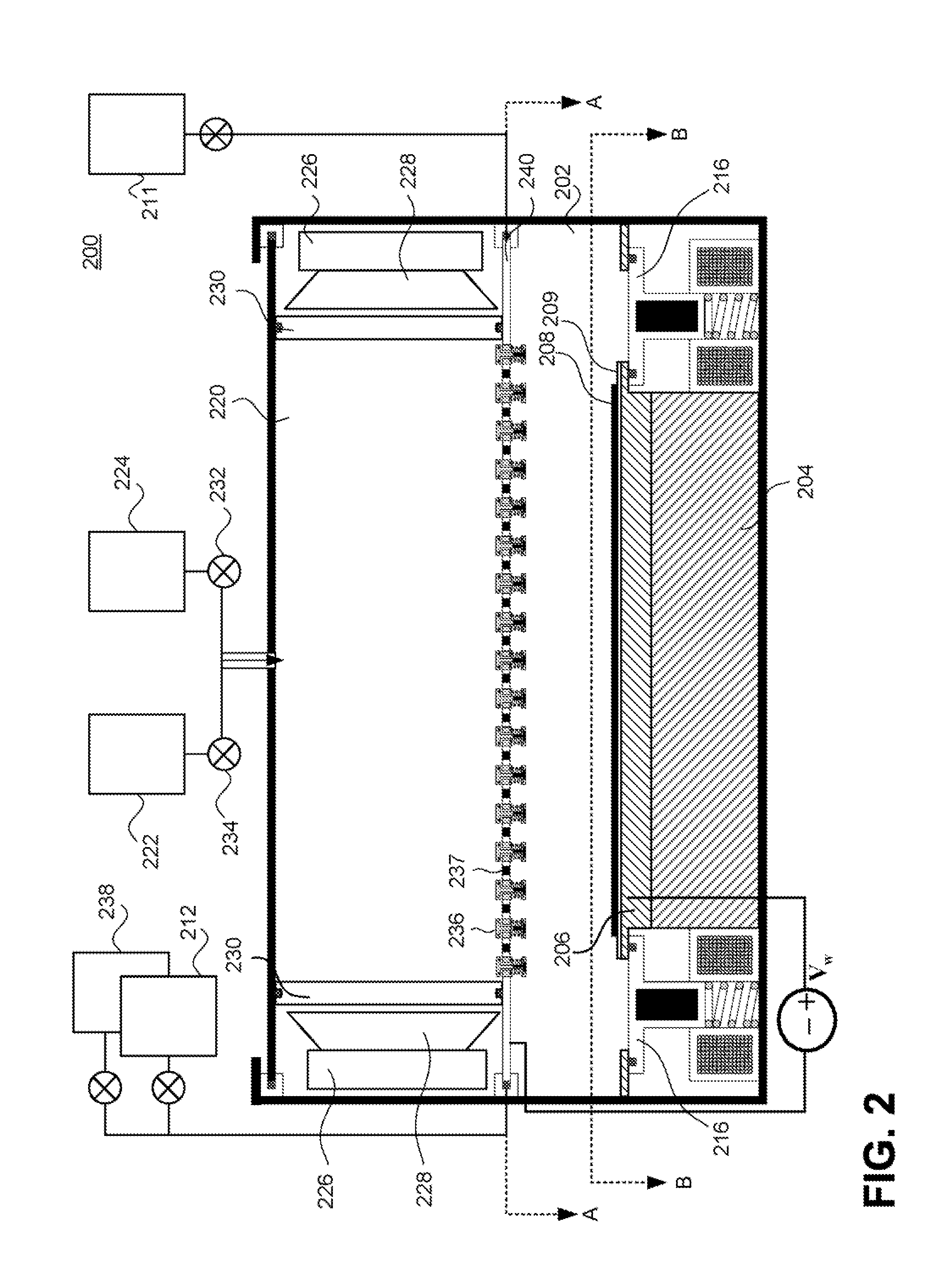
[0045]FIG. 1 depicts a simple ALD process for the deposition of an exemplary Al2O3 film. Substrate 102 has been hydroxylated, resulting in the chemisorption of OH groups on the surface of the substrate. Step 150 depicts a starting surface having OH groups and an inert gas flow. At step 152 of the ALD process, trimethyl aluminum (TMA=Al(CH3)3) is pulsed into the deposition chamber, saturating substrate 102. The TMA is chemisorbed onto the substrate surface, resulting in the deposition of an aluminum containing monolayer (or less) having methyl ligands at the surface. CH4 is liberated during the first step. The deposition chamber is then purged, step 154, to remove any residual precursor or by-products from the chamber. Various means can be employed to purge the chamber, such as by introducing an inert gas into the chamber at inlet port(s) while pumping out the chamber gas through outlet port(s) that are placed downstream of the gas flow. In one embodiment, nitrogen or argon is used a...


PUM

PropertyMeasurementUnit
temperatureaaaaaaaaaa
vacuum pressuresaaaaaaaaaa

Abstract

System and methods for flash heating of materials deposited using atomic layer deposition techniques are disclosed. By flash heating the surface of the deposited material after each or every few deposition cycles, contaminants such as un-reacted precursors and byproducts can be released from the deposited material. A higher quality material is deposited by reducing the incorporation of impurities. A flash heating source is capable of quickly raising the temperature of the surface of a deposited material without substantially raising the temperature of the bulk of the substrate on which the material is being deposited. Because the temperature of the bulk of the substrate is not significantly raised, the bulk acts like a heat sink to aid in cooling the surface after flash heating. In this manner, processing times are not significantly increased in order to allow the surface temperature to reach a suitably low temperature for deposition.

Description

CROSS-REFERENCE TO RELATED APPLICATIONS[0001]The following applications are cross-referenced and incorporated by reference herein in their entirety:[0002]U.S. patent application Ser. No. ______, filed concurrently, entitled “Atomic Layer Deposition of Oxides Using Krypton as an Ion Generating Feed Gas,” by Mokhlesi et al., filed concurrently (Attorney Docket No. SAND-01025US0); and[0003]U.S. patent application Ser. No. ______, filed concurrently, entitled “Systems for Atomic Layer Deposition of Oxides Using Krypton as an Ion Generating Feed Gas,” by Mokhlesi et al., filed concurrently (Attorney Docket No. SAND-01025US1);[0004]U.S. patent application Ser. No. ______, filed concurrently, entitled “Systems for Flash Heating in Atomic Layer Deposition,” by Mokhlesi et al., filed concurrently (Attorney Docket No. SAND-01026US1).BACKGROUND OF THE INVENTION[0005]1. Field of the Invention[0006]The present invention relates generally to technology for atomic layer deposition.[0007]2. Descrip...

Claims


Application Information

Patent Timeline
Patent Type & Authority Applications(United States)
IPC IPC(8): C23C16/00B05D3/00B29C71/04B29C71/02
CPCC23C16/45527H01L29/42324C23C16/45544C23C16/511C23C16/56H01L21/02164H01L21/02178H01L21/02181H01L21/0228H01L21/02345H01L21/02354H01L21/28273H01L21/3141H01L21/3142H01L21/3145H01L21/31612H01L21/3162H01L21/31645H01L27/115H01L27/11521C23C16/45536H01L29/40114H10B69/00H10B41/30
Inventor MOKHLESI, NIMATHAKUR, RANDHIR
Owner SANDISK TECH LLC
Why Eureka
Try Eureka