Fabrication of back-contacted silicon solar cells using thermomigration to create conductive vias

a back-contact silicon and solar cell technology, applied in semiconductor/solid-state device manufacturing, electrical equipment, semiconductor devices, etc., can solve the problems of limited conductivity of laser-drilled vias, limited internal collection depth of photo-generated carriers, and added cost and manufacturing time of laser-drilling steps

Inactive Publication Date: 2007-01-30
ADVENT SOLAR INC +1
View PDF9 Cites 83 Cited by
  • Summary
  • Abstract
  • Description
  • Claims
  • Application Information

AI Technical Summary

Benefits of technology

[0009]Finally, a thermomigrated back-contacted cell can have a more optimally-doped front surface for higher conversion efficiency. In standard front-contacted cells, the front emitter must be doped heavily enough to achieve low contact resistance. Some photocurrent is lost in heavily doped emitters due to increased recombination losses in the emitter. The simplest process sequence for a back-contacted cell using an EWT geometry and laser-drilled holes uses a heavy emitter diffusion to minimize series resistance inside the holes and contact resistance to the grid. In a back-contact cell using thermomigration vias, the front surface n+ diffusion and the conductive via doping can be performed in separate steps—so each step can be separately optimized. Hence, a more optimally-doped front surface comprising a lower doping concentration can be used for thermomigrated cells, which results in increased photocurrent collection.
[0010]Another advantage of thermomigrated vias is lower series resistance. A thermomigrated conductive via provides lower series resistance compared to diffused holes in the EWT cell because it is a solid cylinder that is doped, while the EWT cell only has a thin surface n+ diffusion in the walls of the laser-drilled holes. If the thermomigration metal is left in place after the thermomigration, it should yield a much lower contact resistance, as well. Finally, if the thermomigrated via is a pattern of lines rather than holes, losses due to current flow in the emitter is reduced. Also, if the thermomigrated via pattern is a pattern of lines, the thermomigration metal on the rear surface may be left on the surface and used as the n-type grid.
[0007]Disadvantages of an EWT design that uses laser-drilled holes to make conductive vias is the need for drilling a large number of holes (e.g., 600 holes / in2), and the added cost and manufacturing time of performing the laser-drilling step. Additionally, the conductivity of the laser-drilled vias may be limited by the achievable concentration of n-type dopant, and by the depth of the emitter diffusion layer realized on the interior surfaces of the laser-drilled holes. In other words, the performance of laser-drilled / diffused EWT cells is limited by the need to perform a single heavy diffusion to achieve sufficiently high conductivity in the laser-drilled vias.

Problems solved by technology

An important issue for back-contacted silicon solar cells is identifying a cell design and fabrication process that are inexpensive to manufacture and that can use inexpensive, lower-quality silicon substrates.
Solar cells that use inexpensive silicon substrates contain greater amounts of impurities and crystalline defects, which limit the internal collection depth of photo-generated carriers.
Disadvantages of an EWT design that uses laser-drilled holes to make conductive vias is the need for drilling a large number of holes (e.g., 600 holes / in2), and the added cost and manufacturing time of performing the laser-drilling step.
Additionally, the conductivity of the laser-drilled vias may be limited by the achievable concentration of n-type dopant, and by the depth of the emitter diffusion layer realized on the interior surfaces of the laser-drilled holes.
In other words, the performance of laser-drilled / diffused EWT cells is limited by the need to perform a single heavy diffusion to achieve sufficiently high conductivity in the laser-drilled vias.
Some photocurrent is lost in heavily doped emitters due to increased recombination losses in the emitter.
However, this technique has not been used to fabricate completely back-contacted solar cells.
Unacceptably large temperature variations would create non-uniform annealing rates, diffusion rates, etc. and may result in poor reliability, reduced yield, etc.

Method used


Image

  • Fabrication of back-contacted silicon solar cells using thermomigration to create conductive vias
  • Fabrication of back-contacted silicon solar cells using thermomigration to create conductive vias
  • Fabrication of back-contacted silicon solar cells using thermomigration to create conductive vias

Examples


Embodiment Construction

[0026]Note that in the drawings, the thicknesses of the various layers of insulating, semiconducting, and metallic materials; and other dimensions, such as the width of contact pads, are not drawn to scale, but, rather, are shown schematically for purposes of illustration and easy identification.

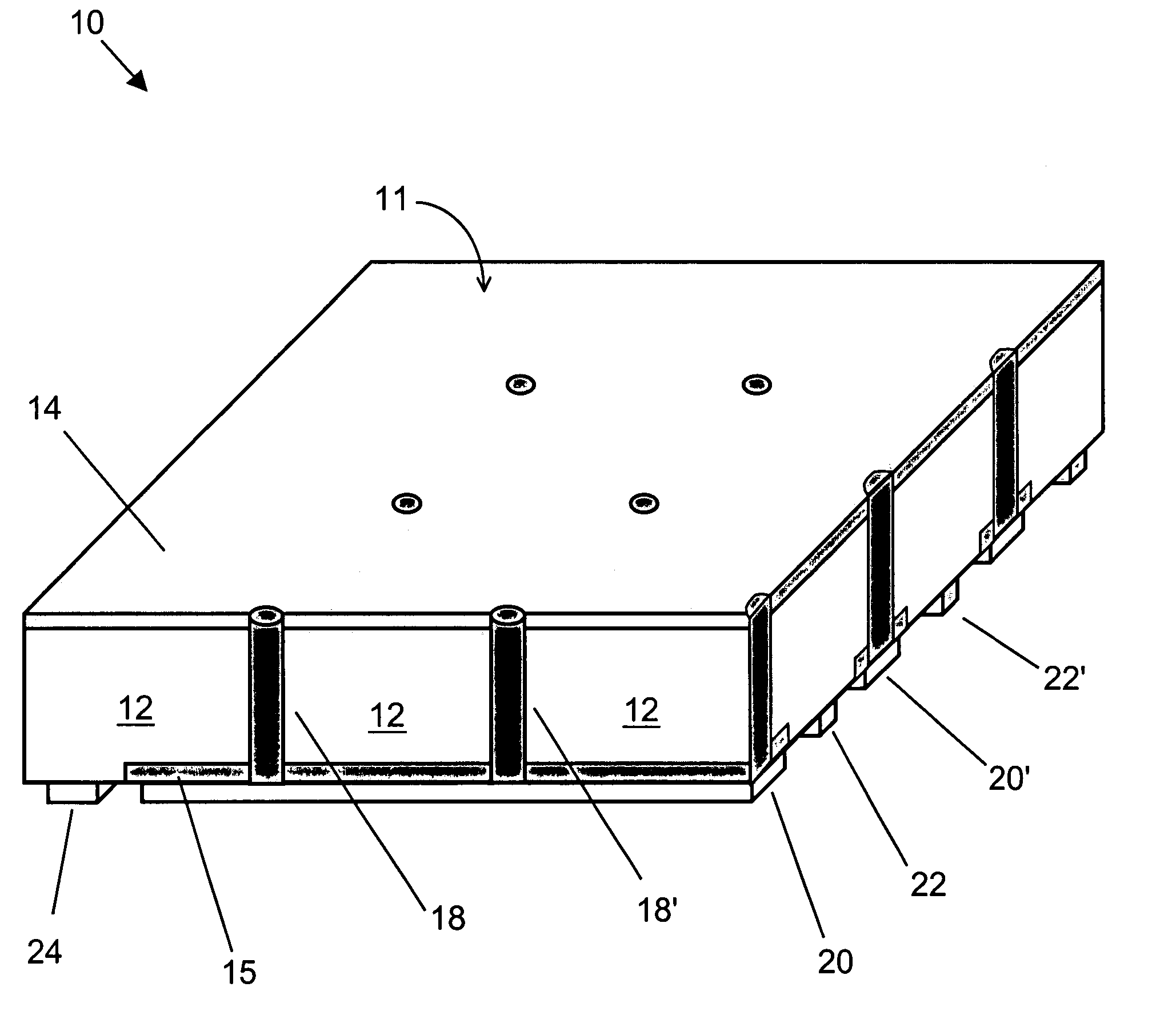
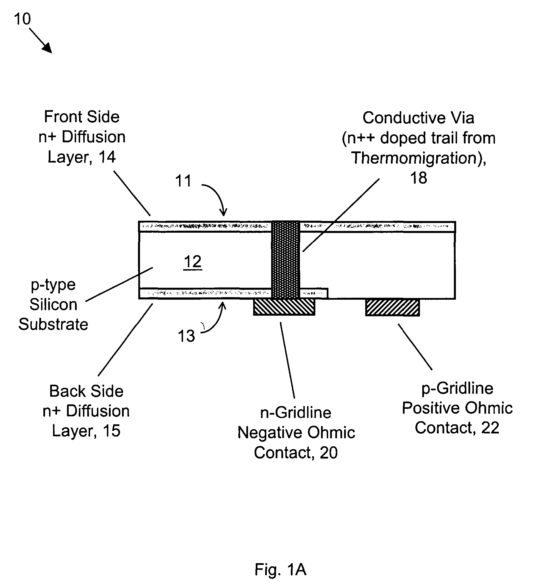
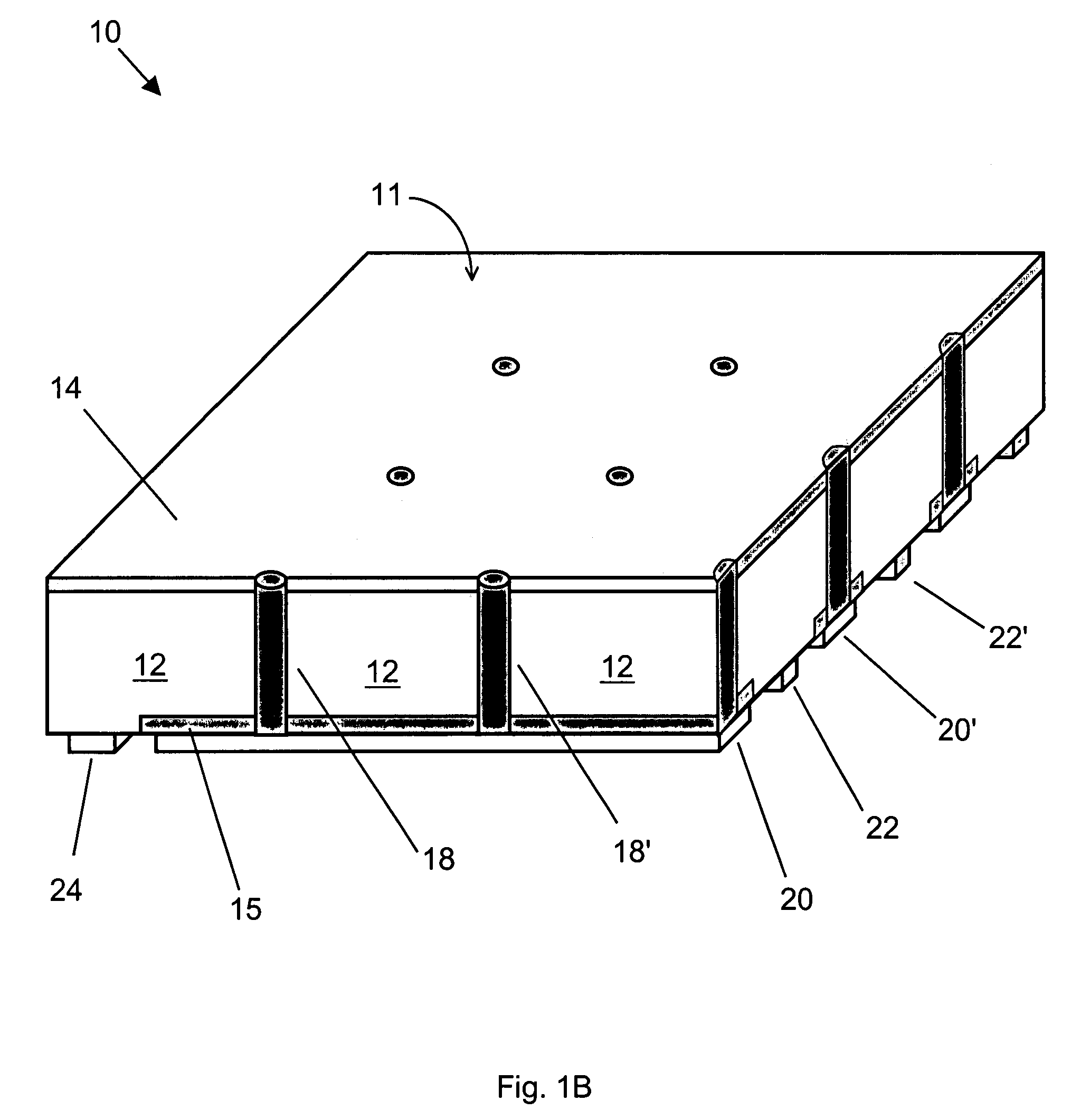
[0027]FIG. 1A shows a schematic cross-section side view of a first example of a back-contacted silicon solar cell, according to the present invention. Back-contacted solar cell 10 comprises a p-type bulk silicon substrate 12; a front side n+ diffusion emitter layer 14 located on the front side 11 of substrate 12; a backside n+ diffusion emitter layer 15 located on the backside 13 of substrate 12; a n-gridline negative ohmic contact 20 located on the backside 13 of substrate 12, contacting backside emitter layer 15; a n++ conductive via 18 disposed through the thickness of substrate 12 that electrically connects front side emitter layer 14 to negative ohmic contact 20 located on backside 13 a...


PUM


Abstract

Methods of manufacturing back-contacted silicon solar cells fabricated using a gradient-driven solute transport process, such as thermomigration or electromigration, to create n-type conductive vias connecting the n-type emitter layer on the front side to n-type ohmic contacts located on the back side.

Description

FEDERALLY SPONSORED RESEARCH[0001]The United States Government has rights in this invention pursuant to Department of Energy Contract No. DE-AC04-94AL85000 with Sandia Corporation.CROSS-REFERENCE TO RELATED APPLICATIONS[0002]NoneBACKGROUND OF THE INVENTION[0003]The present invention relates generally to methods of manufacturing photovoltaic silicon solar cells, and more specifically to back-contacted solar cells fabricated using a gradient-driven migration process, such as thermomigration or electromigration, to create an array of n++ conductive vias electrically connecting an n+ emitter surface on the front side of the cell to a grid of ohmic contacts located on the cell's backside.[0004]Back-contacted silicon solar cells (photovoltaic cells) have several advantages compared to traditional silicon solar cells that have ohmic contacts located on both the front and rear surfaces. One advantage is that back-contacted cells have a higher conversion efficiency due to reduced (or elimina...

Claims


Application Information

Patent Timeline
Patent Type & Authority Patents(United States)
IPC IPC(8): H01L31/04H01L21/768H01L31/00H01L31/0224H01L31/05H01L31/068H01L31/18
CPCH01L21/76898H01L31/022458Y02E10/50Y02E10/547
Inventor GEE, JAMES MSCHMIT, RUSSELL R.
Owner ADVENT SOLAR INC
Why Eureka
Try Eureka