

Cis Compound Semiconductor Thin-Film Solar Cell and Method of Forming Light Absorption Layer of the Solar Cell
a solar cell and compound semiconductor technology, applied in the direction of sustainable manufacturing/processing, climate sustainability, semiconductor devices, etc., can solve the problems of high cost, complex and expensive film formation apparatus, and difficult to ensure uniformity throughout a large area of multi-source deposition, so as to reduce production energy cost, improve productivity, and high conversion efficiency
- Summary
- Abstract
- Description
- Claims
- Application Information
AI Technical Summary
Benefits of technology
Problems solved by technology
Method used
Image

Examples
Embodiment Construction
[0020] Embodiments of the invention will be explained below.
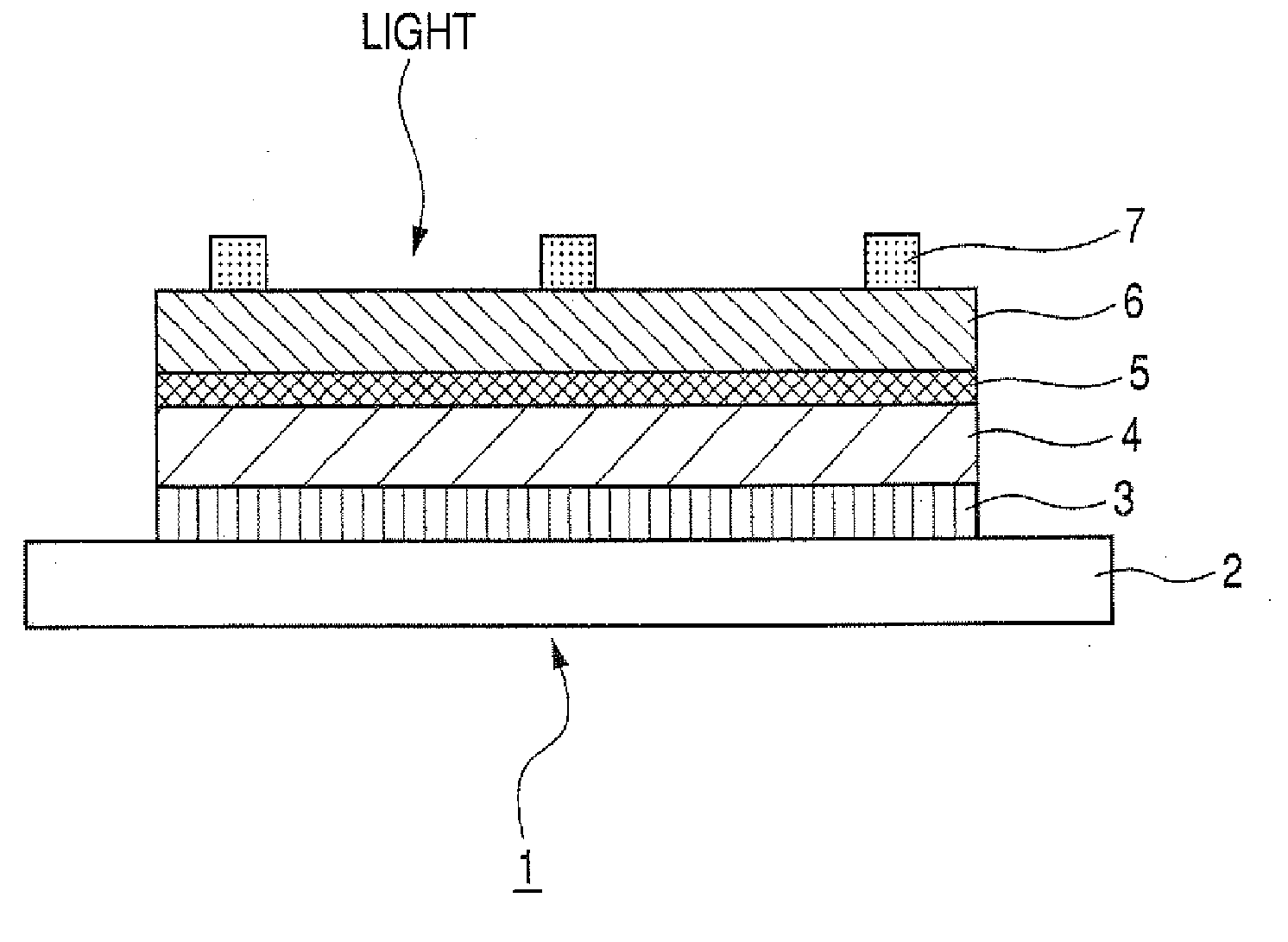
[0021] First, the basic structure of the CIS compound semiconductor thin-film solar cell 1 is a multilayer structure which, as shown in FIG. 4, comprises a substrate 2 and, superposed thereon in the following order, a metallic back electrode 3, a light absorption layer 4, an interfacial layer (buffer layer) 5, a window layer 6, and an upper electrode 7. The metallic back electrode 3 formed on the glass substrate 2 is a highly corrosion-resistant metal having a high melting point, e.g., molybdenum or titanium, which has a thickness of 1-2 μm. The light absorption layer 4 is a thin film of a CIS compound semiconductor showing p-type conduction, and it has a thickness of 1-3 μm. Namely, the light absorption layer is constituted of a Cu-III-VI2 Group chalcopyrite (type) semiconductor, e.g., copper indium diselenide (CIS), copper indium gallium diselenide (CIGS), or copper indium gallium diselenide sulfide (CIGSS), or CIGS havi...
PUM
 Abstract
Description
Claims
Application Information