Hybrid photovoltaic device

a photovoltaic device and hybrid technology, applied in the direction of semiconductor devices, electrical devices, nanotechnology, etc., can solve the problems of high-efficiency photovoltaic devices mainly using single crystalline materials, low efficiency of photovoltaic devices, and low so as to improve the collection of sunlight, reduce the cost of photovoltaic power generation, and absorb more sunlight

Active Publication Date: 2009-07-02
BANPIL PHOTONICS
View PDF7 Cites 105 Cited by
  • Summary
  • Abstract
  • Description
  • Claims
  • Application Information

AI Technical Summary

Benefits of technology

[0020]One objective of this invention is to provide a design of a photovoltaic device that exhibits improved collection of the sunlight, thereby absorbing more sunlight from the solar spectrum. Accordingly, a hybrid photovoltaic device (hereinafter hybrid device) disclosed in this invention utilizes a plurality of nanostructures (hereinafter nanostructures) embedded in a matrix of another material exhibiting photovoltaic effect, including but not limited to crystalline semiconductor, amorphous semiconductor, photosensitive polymers and / or a combination thereof. A combination of different materials in the nanostructures and the matrix allows collection of light from different sections of the solar spectrum. Large effective surface area to volume ratio of the plurality of nanostructures of the hybrid device according to the principles of the invention is advantageous.
[0021]A second objective of this invention is to provide a photovoltaic device that exhibits high conversion efficiency. Accordingly, a hybrid device disclosed in this invention utilizes III-V alloy semiconductor nanostructures comprising a plurality of cylinders, or pillars, vertically projecting upwards from a substrate, embedded in a matrix of another semiconductor exhibiting photovoltaic effect, including crystalline, microcrystalline or polycrystalline semiconductor, and / or amorphous semiconductor. Advantageously, such a structure absorbs photon flux from a larger section of the solar spectrum thereby, improving efficiency of collection and conversion of the photon energy into electrical energy. An exemplary system according to the principles of this invention utilizes indium phosphide (InP) nanostructures embedded in a matrix of a-Si.
[0022]A third objective is to provide a design of a photovoltaic device that effectively utilizes the large reflectivity of semiconductor surfaces. Accordingly, one example of a hybrid device disclosed in this invention utilizes III-V alloy semiconductor nanostructures comprising a plurality of tapered cylinders embedded in a matrix of a-Si, such that the photon flux incident on the tapered surface of the plurality of tapered cylinders along the length, reflect a portion of the photon flux into the matrix of a-Si thereby, increasing the effective photon flux incident upon the matrix of a-Si.

Problems solved by technology

A major fraction of cost of generating photovoltaic power lies in manufacturing photovoltaic devices and modules.
The cost of manufacturing photovoltaic devices mainly depends on the materials as well as processing cost.
For example, high efficiency photovoltaic devices that mainly utilize single crystalline materials such as, crystalline silicon (c-Si), poly-crystalline silicon (poly-Si), III-V alloy semiconductors including but not limited to, GaAs, InP, GaAlAs, GaInAsP, GaInAs, and their combinations thereof in single or multiple homojunctions, heterojunctions, or tandem photovoltaic devices are the most expensive ones.
However, these types of photovoltaic devices are not cost effective in power generation for terrestrial applications such as residential, industrial, and commercial power generation that require better reliability and higher efficiency than applications in consumer electronics.
While other low cost materials, such as II-VI semiconductors including but not limited to, cadmium sulfide (CdS) / cadmium telluride (CdTe) and copper indium diselenide (CIS) are useful for photovoltaic devices, they have adverse environmental impact, and are therefore not a viable choice for ‘clean energy’.

Method used


Image

  • Hybrid photovoltaic device
  • Hybrid photovoltaic device
  • Hybrid photovoltaic device

Examples


Embodiment Construction

[0045]This invention was first presented as a proposal (Phase-I SBIR Proposal # 0741061) for a research grant to National Science Foundation on Jun. 13, 2007. The principles of the invention may be appreciated by the description of exemplary embodiments disclosed in the specification in view of the accompanying drawing FIGS. 3-11 in which like parts are indicated by like reference numerals in all the drawing figures to avoid repetitions in describing them.

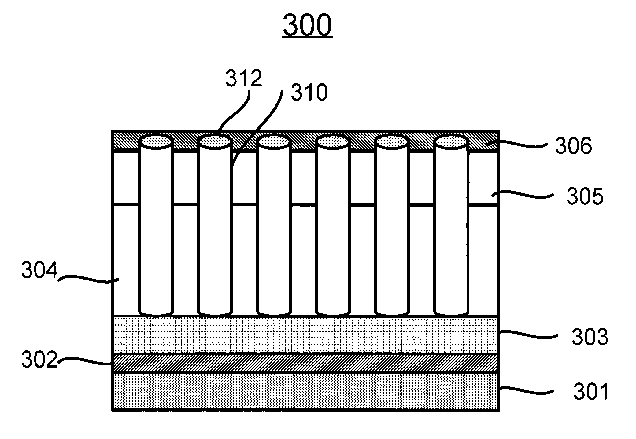
[0046]FIG. 3A shows a cross sectional view (300) of an exemplary planar hybrid device according to the principles of the invention. The device structure is similar to that of a conventional planar a-Si device shown earlier in FIG. 2, wherein like parts are indicated with like reference numerals. More specifically, the hybrid device (300) constructed on a substrate (301) comprises multiple layers including a transparent conductor layer (302), a first layer (303), a plurality of nanostructures represented as 310, (only one nanostruct...


PUM


Abstract

A hybrid photovoltaic device comprising a plurality of nanostructures embedded in a matrix of a photosensitive material including one or more layers. A combination of innovative structural aspects of the hybrid photovoltaic device results in significant improvements in collection of incident light from the solar spectrum, better absorption of light, and better collection of the photo-carriers generated in response to the incident light, thereby improving efficiency of the hybrid photovoltaic device.

Description

CROSS-REFERENCE TO RELATED APPLICATIONS[0001]Not ApplicableSTATEMENT REGARDING FEDERALLY SPONSORED RESEARCH OR DEVELOPMENT[0002]Not Applicable.FIELD OF THE INVENTION[0003]This invention is related to photovoltaic power generation, and in particular to photovoltaic power generation in a multilayered hybrid photovoltaic device comprising a nanostructure embedded in a matrix of another material exhibiting photovoltaic effect. The hybrid photovoltaic device integrates conventional nanostructure technology with the conventional photovoltaic device technology for high efficiency.BACKGROUND OF THE INVENTION[0004]Photovoltaic power generation is considered as an alternative for conventional power generation, for example from fossil fuels and nuclear energy. It is particularly vied for its minimal environmental impact as a ‘clean energy’ source. Photovoltaic power is generated in a photovoltaic device, popularly known as a solar cell. In order for photovoltaic power generation to be viable a...

Claims


Application Information

Patent Timeline
Patent Type & Authority Applications(United States)
IPC IPC(8): H01L31/028H01L31/0272H01L31/0304H01L31/0296
CPCH01L31/0296Y02E10/547H01L31/035281H01L31/03529H01L31/03682H01L31/03685H01L31/03762H01L31/068H01L31/0687H01L31/0693H01L31/072H01L31/0725H01L31/073H01L31/0735H01L31/075H01L31/076H01L31/077Y02E10/543Y02E10/544Y02E10/548Y02E10/545Y02E10/546Y10S977/948H01L31/0304H01L31/035227
Inventor DUTTA, ACHYUT KUMAR
Owner BANPIL PHOTONICS
Why Eureka
Try Eureka