Method of manufacturing oxide superconductive wire

a superconductive wire and oxide technology, applied in the direction of superconducting magnets/coils, superconductor devices, magnetic bodies, etc., can solve the problem of difficult to maintain crystal orientation in the same direction, and achieve the effect of superior critical current density

Inactive Publication Date: 2007-05-24
SUMITOMO ELECTRIC IND LTD
View PDF6 Cites 0 Cited by
  • Summary
  • Abstract
  • Description
  • Claims
  • Application Information

AI Technical Summary

Benefits of technology

[0015] According to the present invention, a method of manufacturing an oxide superconductive wire which can attain a superior critical current density can be provided.

Problems solved by technology

It is because, when the oxide superconductive wire is made long, an oxide used becomes long, which makes it difficult to maintain crystal orientation in the same direction.

Method used


Image

  • Method of manufacturing oxide superconductive wire
  • Method of manufacturing oxide superconductive wire

Examples


example 1

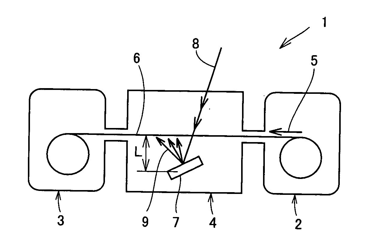
[0033] An orientation substrate of an Ni group alloy (0.1 mm thickness×10 mm width ×50 m length) having yttria-stabilized zirconia (YSZ) of a thickness of 1 μm deposited thereon as an intermediate layer was prepared. On this substrate, an oxide superconductive layer of HoBa2Cu3O7-x (HoBCO) was deposited. As a manufacturing condition, a laser deposition method was used with laser energy of 600 mJ. Oxygen was used as a film formation gas, a gas pressure was set to 26.7 kPa (200 Torr), and a distance between a deposition object (metal tape) and a target was kept 80 mm. An irradiation area on the target was set to 4 mm×6 mm with a condenser lens to form a rectangular plume.

[0034] In the condition as described above, a Hastelloy tape as above was transferred through the plume to form a film with adjusting a frequency of a laser so as to obtain a desired thickness of 0.25 μm over a whole film. A sample as a reference was prepared by a method in which a superconductive film was deposited ...

example 2

[0036] The orientation substrate of the Ni group alloy used in example 1 which had the intermediate layer deposited thereon was used, and an HoBCO film was deposited thereon as in example 1. As a manufacturing condition, the distance between the deposition object (metal tape) and the target was changed to 60 mm, and the irradiation area on the target was set to 0.6 mm×40 mm with a condenser lens to form a line plume. The other conditions were made similar to those in example 1.

[0037] In example 2, the oxide superconductive layer was formed at respective four transfer speeds of 1.7 m / h, 2.5 m / h, 5 mh, and 6.6 m / h to obtain samples. Critical current values (Ic) of the samples were measured. A critical current density (Jc) was measured using the Ic obtained. Results are shown in Table 2. Table 2 indicates that, in example 2, there is also a tendency of the Jc to increase as the transfer speed increases, as in example 1. In particular, the value of Jc increased at the transfer speed of...


PUM

PropertyMeasurementUnit
distanceaaaaaaaaaa
transfer speedaaaaaaaaaa
thicknessaaaaaaaaaa

Abstract

A method of manufacturing an oxide superconductive wire includes the step of positioning a metal tape in a position at a distance (L) of at most 100 mm from a target for generating an oxide, and the step of forming an oxide superconductive layer on the metal tape using a vapor deposition method while transferring the metal tape at a transfer speed of at least 5 m / h with keeping the distance (L) between the metal tape and the target of at most 100 mm.

Description

TECHNICAL FIELD [0001] The present invention relates to a method of manufacturing an oxide superconductive wire. More specifically, the present invention relates to a method of manufacturing an oxide superconductive wire including an oxide superconductive layer deposited on a metal tape. BACKGROUND ART [0002] An oxide superconductive wire has a characteristic that a critical current density (Jc) of at least 1 MA / cm2 can be obtained at a relatively high temperature (77 K) as compared to other superconductive materials, and therefore expectations for mass production thereof are rising. [0003] In a conventional technique, a Jc larger than 1 MA / cm2 is already attained with a superconductive wire having a short length. With the oxide superconductive wire having a long length, however, a technique for attaining the Jc of at least 1 MA / cm2 should be developed from now on. [0004] A reason why the Jc cannot be increased in the oxide superconductive wire having a long length is described here...

Claims


Application Information

Patent Timeline
Patent Type & Authority Applications(United States)
IPC IPC(8): B05D5/12H01L39/24C23C14/28C23C14/08H01B12/06H01B13/00H01F6/06H10N60/01
CPCH01L39/2448H10N60/0521H01B13/0026H01B12/06H10N60/0801H10N60/0296
Inventor HAHAKURA, SHUJIOHMATSU, KAZUYAKONISHI, MASAYAFUJINO, KOSO
Owner SUMITOMO ELECTRIC IND LTD
Why Eureka
Try Eureka