Memory devices including floating body transistor capacitorless memory cells and related methods

a memory cell and capacitorless technology, applied in the field of memory devices including related methods, can solve the problems of volatile nature of floating body transistor capacitorless memory cells, prone to read errors, and prone to errors in reading

Inactive Publication Date: 2007-06-07
SAMSUNG ELECTRONICS CO LTD
View PDF18 Cites 40 Cited by
  • Summary
  • Abstract
  • Description
  • Claims
  • Application Information

AI Technical Summary

Benefits of technology

The present invention is about a semiconductor memory device that includes a memory cell array with multiple unit memory cells. Each unit memory cell consists of complementary first and second floating body transistor capacitor-less memory cells. The technical effect of this invention is to provide a more efficient and compact semiconductor memory device with improved performance and reliability.

Problems solved by technology

The technical problem addressed in this patent text is the occurrence of reading errors in floating body transistor capacitor-less memory cells and the need for a reference current generator, reference memory cells, and other circuits to generate the reference current. These issues can limit the density of the memory device and increase the time required for refresh operations.

Method used


Image

  • Memory devices including floating body transistor capacitorless memory cells and related methods
  • Memory devices including floating body transistor capacitorless memory cells and related methods
  • Memory devices including floating body transistor capacitorless memory cells and related methods

Examples


Embodiment Construction

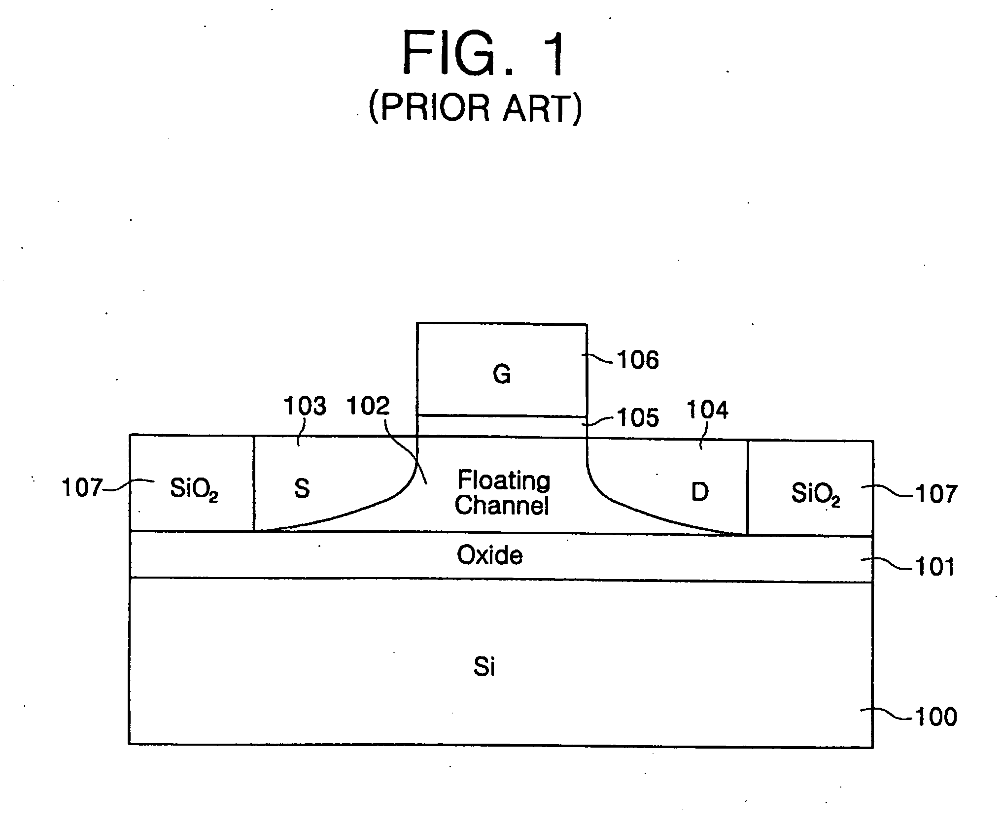
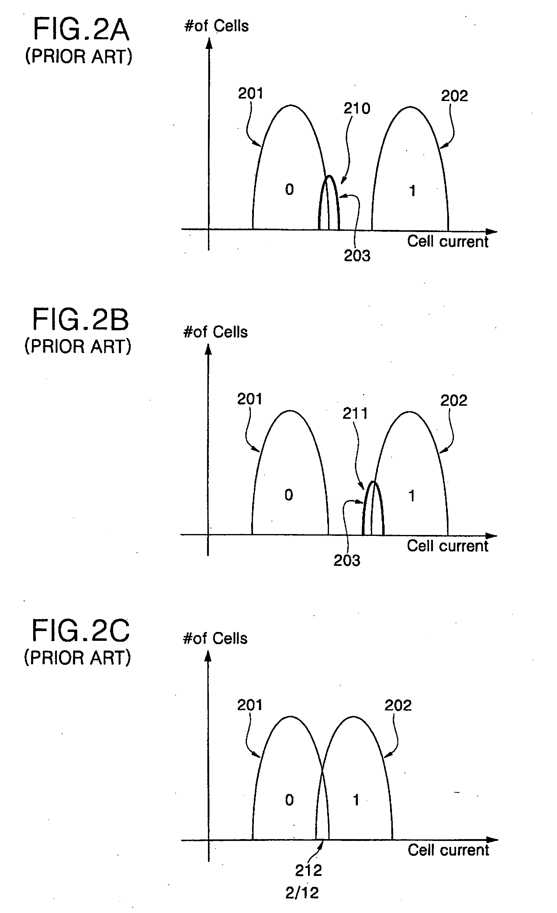
[0034] The invention is described more fully hereinafter with reference to the accompanying drawings, in which exemplary embodiments of the present invention are shown. The present invention may, however, be embodied in many different forms and should not be construed as limited to the examples set forth herein. In the drawings, the sizes and relative sizes of layers and regions may be exaggerated and / or simplified for clarity. Also, it will be understood that when an element or layer is referred to as being “on”, “connected to” or “coupled to” another element or layer, it can be directly on, connected or coupled to the other element or layer, or intervening elements or layers may be present.

[0035] The present invention will now be described by way of preferred, but non-limiting, embodiments of the invention.

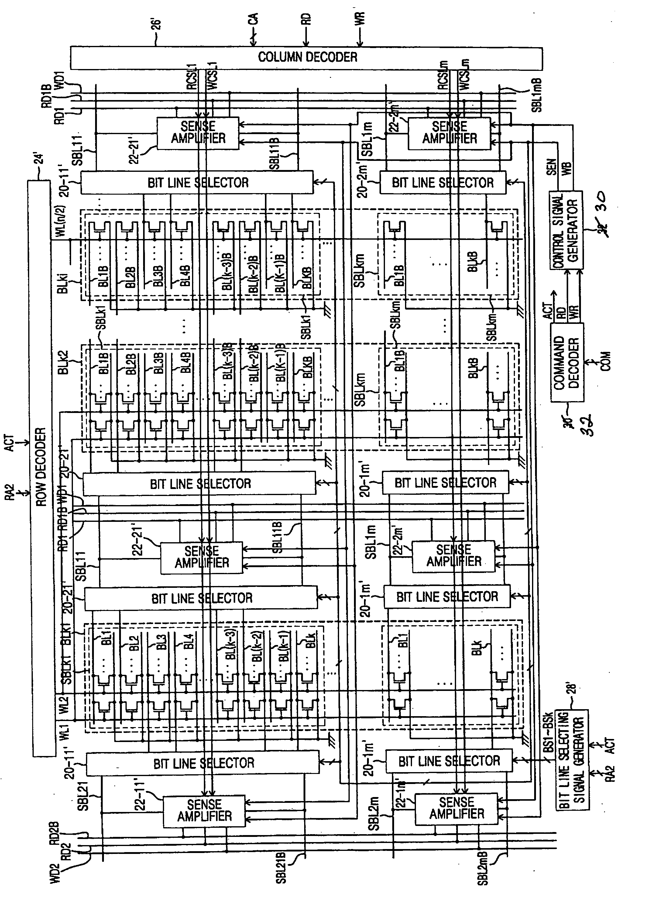
[0036]FIG. 3 is a block diagram of floating body transistor capacitorless memory cell memory device according to an embodiment of the present invention.

[0037] The memory devi...


PUM


Abstract

A semiconductor memory device includes a memory cell array which includes a plurality of unit memory cells, where each of the unit memory cells comprises complementary first and second floating body transistor capacitor-less memory cells. A logic value written into and read from each unit memory cell is defined by a difference in threshold voltage states of the first and second floating body transistor capacitorless memory cells.

Description


Claims


Application Information

Patent Timeline
Owner SAMSUNG ELECTRONICS CO LTD
Why Eureka
Try Eureka