Data processing system and nonvolatile memory

a data processing system and non-volatile memory technology, applied in static storage, digital storage, instruments, etc., can solve problems such as depletion of state, and achieve the effect of reducing the number of second loops and reducing the total overhead time resulting from loop switching

Active Publication Date: 2007-06-14
RENESAS ELECTRONICS CORP
View PDF4 Cites 3 Cited by
  • Summary
  • Abstract
  • Description
  • Claims
  • Application Information

AI Technical Summary

Benefits of technology

[0007] It is therefore an object of the present invention to provide a semiconductor integrated circuit which allows erasing to a nonvolatile memory cell without causing depletion halfway through the erase operation.
[0021] By detecting the state of erase voltage application till immediate before the nonvolatile memory cell having a fast erase characteristic is brought into the over-erased state in the first loop and reflecting the detected state on the application of the erase voltage in the subsequent erase / verify loop (second loop), the number of second loops can be reduced and the total overhead time resulting from loop switching can be reduced. This allows high-speed erasing of the nonvolatile memory cell without causing depletion halfway therethrough.

Problems solved by technology

However, if the write-back process cannot be completed due to the shutdown of an operating power source halfway through the erase operation or the like, the depleted state remains.
There is a risk that the problem becomes apparent when such a nonvolatile memory is mounted on an IC card or a memory card which supports hot plug.

Method used


Image

  • Data processing system and nonvolatile memory
  • Data processing system and nonvolatile memory
  • Data processing system and nonvolatile memory

Examples


Embodiment Construction

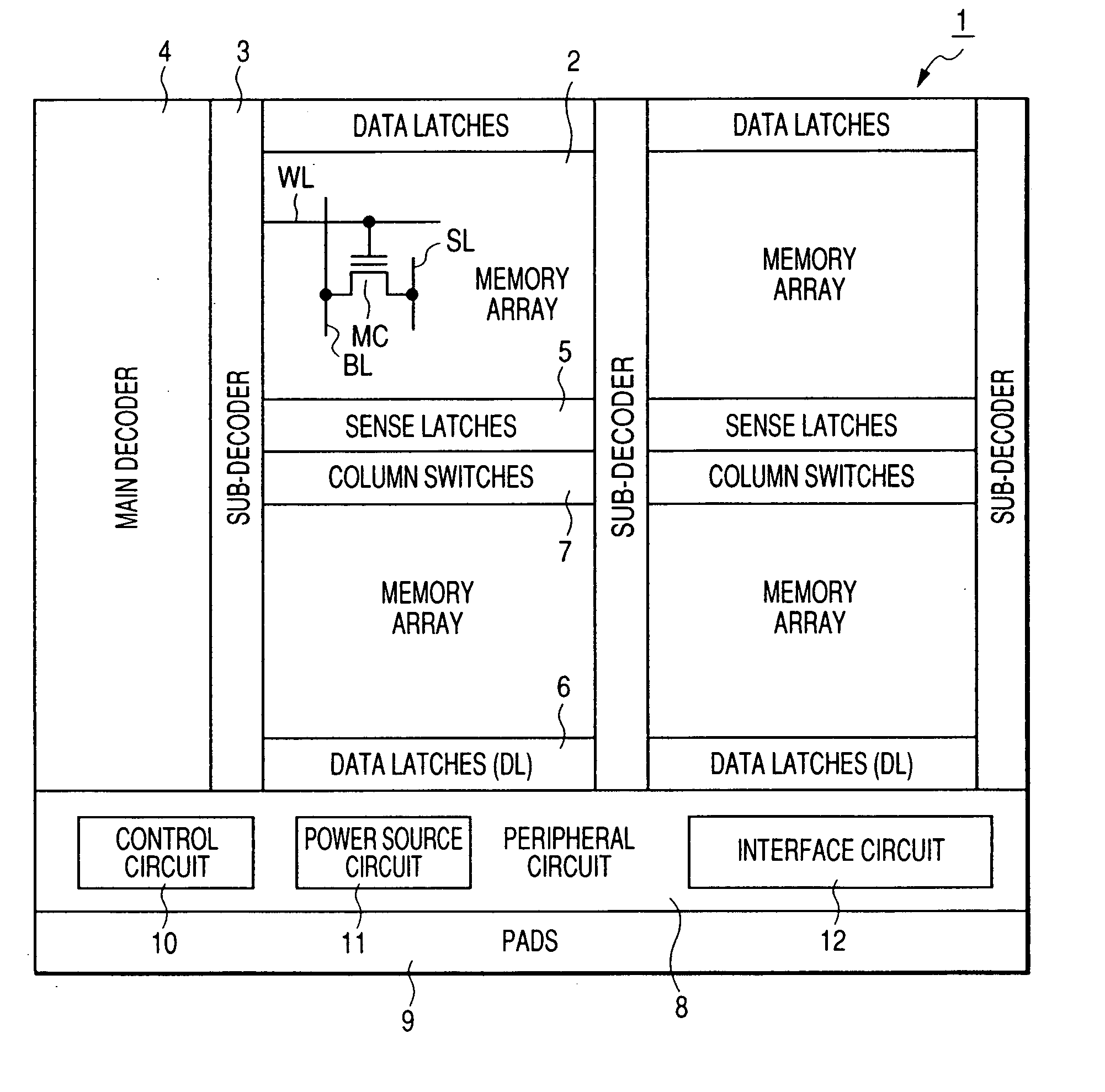
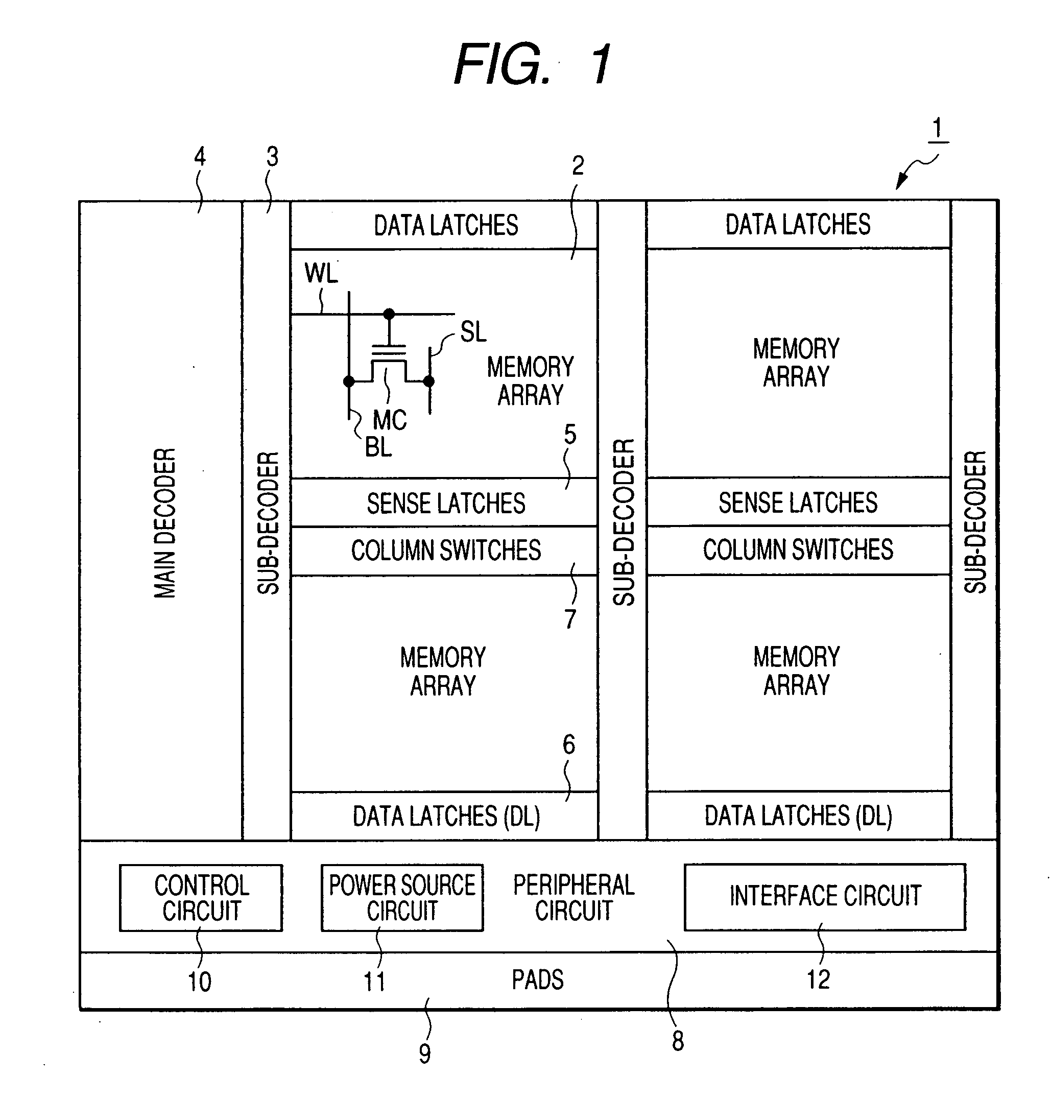
[0039]FIG. 1 shows a flash memory 1 according to an example of the present invention. The flash memory 1 is formed on a single semiconductor substrate made of single-crystal silicon or the like and comprises: a memory array 2; a sub-decoder 3; a main decoder 4; sense latches 5; data latches 6; column switches 7; peripheral circuits 8; and pads 9. The peripheral circuits 8 include: a power source circuit 11; a control circuit 10; and an interface circuit 12.

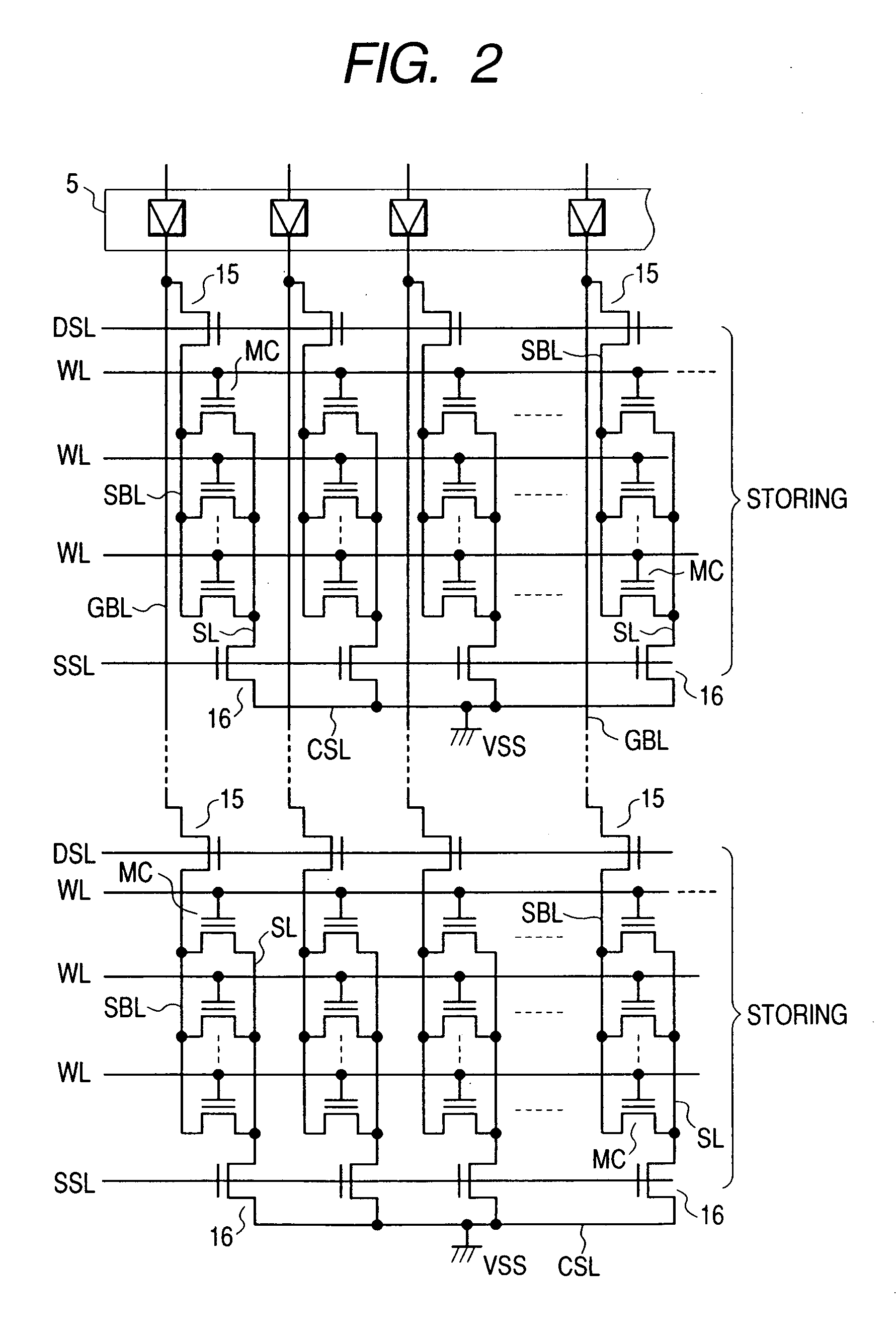
[0040] The foregoing memory array 2 has a large number of nonvolatile memory cells MC each having a threshold voltage which can be changed reversibly by electrical erasing and writing. In the present specification, erasing indicates lowering the threshold voltage of each of the nonvolatile memory cells MC and writing indicates increasing the threshold voltage of the nonvolatile memory cell. The nonvolatile memory cell MC has, e.g., a stacked gate structure having a floating gate and a control gate insulated from each other over a...


PUM


Abstract

Erasing is performed with respect to a nonvolatile memory cell without causing depletion halfway therethrough. A control circuit for reversibly and variably controlling the threshold voltage of the nonvolatile memory cell by electrical erasing and writing controls an erase process of performing erasing to the plurality of nonvolatile memory cells assigned to one unit in an erase operation, a first write process of performing writing to the nonvolatile memory cell exceeding a pre-write-back level before a depletion level, and a second write process of performing writing to the nonvolatile memory cell exceeding a write-back level after the first write process. Since the occurrence of depletion is suppressed by successively performing the first write process with respect to the nonvolatile memory cells which may exceed the depletion level in the erase process, erasing can be performed to the nonvolatile memory cell without causing depletion halfway therethrough.

Description

CROSS-REFERENCE TO RELATED APPLICATION [0001] The present application claims priority from Japanese Patent Application JP 2003-302334 filed on Aug. 27, 2003, the content of which is hereby incorporated by reference into this application. BACKGROUND OF THE INVENTION [0002] The present invention relates to a semiconductor integrated circuit having nonvolatile memory cells each having a threshold voltage which can be changed reversibly by electrical erasing and writing and, more particularly to a technology for suppressing the over-erasing of the nonvolatile memory cell. [0003] The foregoing nonvolatile memory cell has an erased state and a written state. The erased state is, e.g., a state in which a threshold voltage viewed from the select terminal of the memory cell is low and the written state is, e.g., a state in which the threshold voltage viewed from the select terminal of the memory cell is high. The select terminal of the nonvolatile memory cell is connected to a word line and ...

Claims


Application Information

Patent Timeline
Patent Type & Authority Applications(United States)
IPC IPC(8): G11C16/04G11C16/02G11C16/00G11C16/14G11C16/34
CPCG11C16/3468G11C16/00G11C16/04G11C16/14G11C16/34
Inventor MATSUBARA, KENTAKASE, YOSHINORIFUJISAWA, TOMOYUKI
Owner RENESAS ELECTRONICS CORP
Why Eureka
Try Eureka