Igbt cathode design with improved safe operating area capability

Active Publication Date: 2007-07-12
HITACHI ENERGY SWITZERLAND AG
View PDF6 Cites 8 Cited by
  • Summary
  • Abstract
  • Description
  • Claims
  • Application Information

AI Technical Summary

Problems solved by technology

Firstly, it efficiently co...

Method used


Image

  • Igbt cathode design with improved safe operating area capability
  • Igbt cathode design with improved safe operating area capability
  • Igbt cathode design with improved safe operating area capability

Examples


Embodiment Construction

[0008] It is an object of the invention to provide an insulated gate semiconductor device of the type mentioned initially that overcomes the deficiencies mentioned above.

[0009] This object is achieved by an insulated gate semiconductor device according to claim 1.

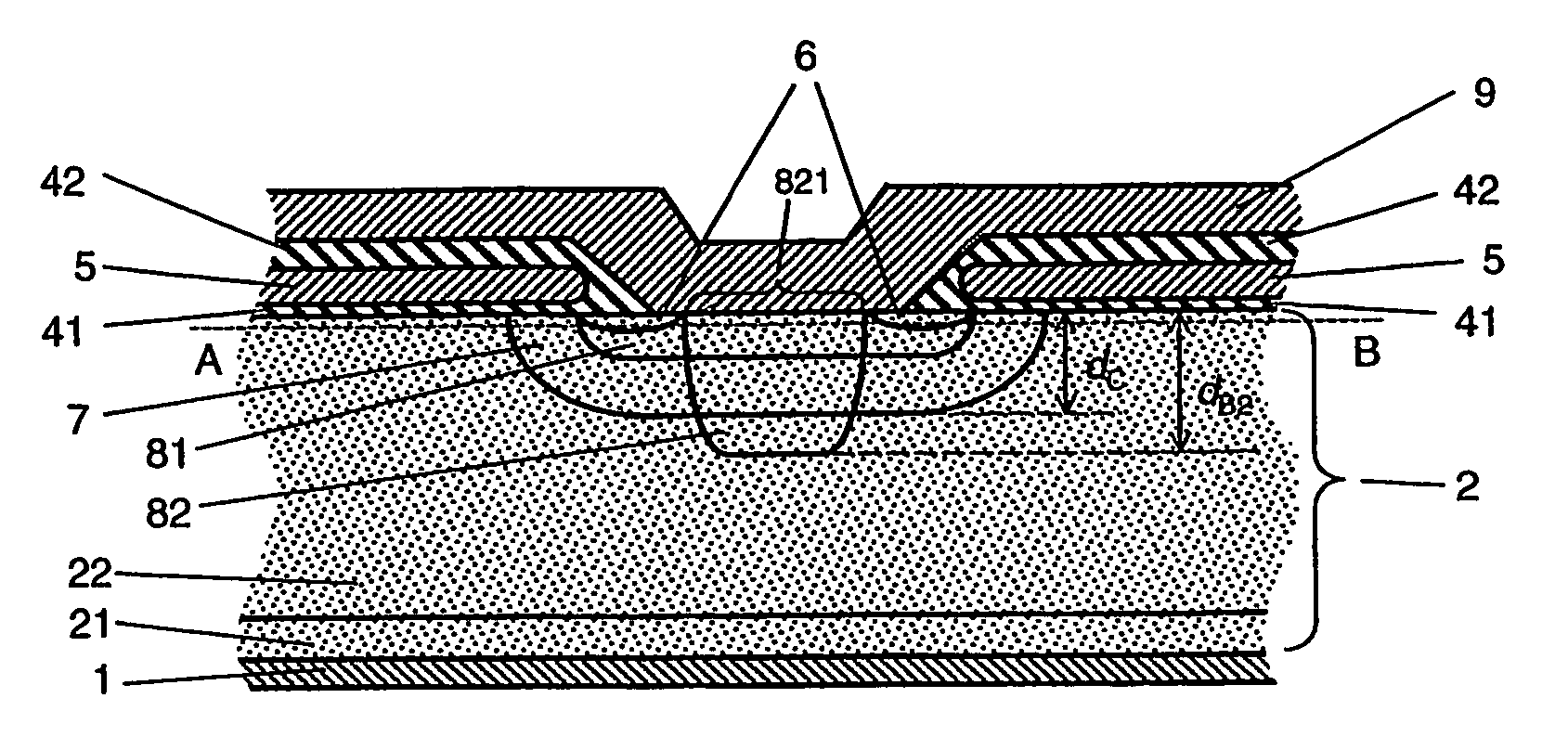
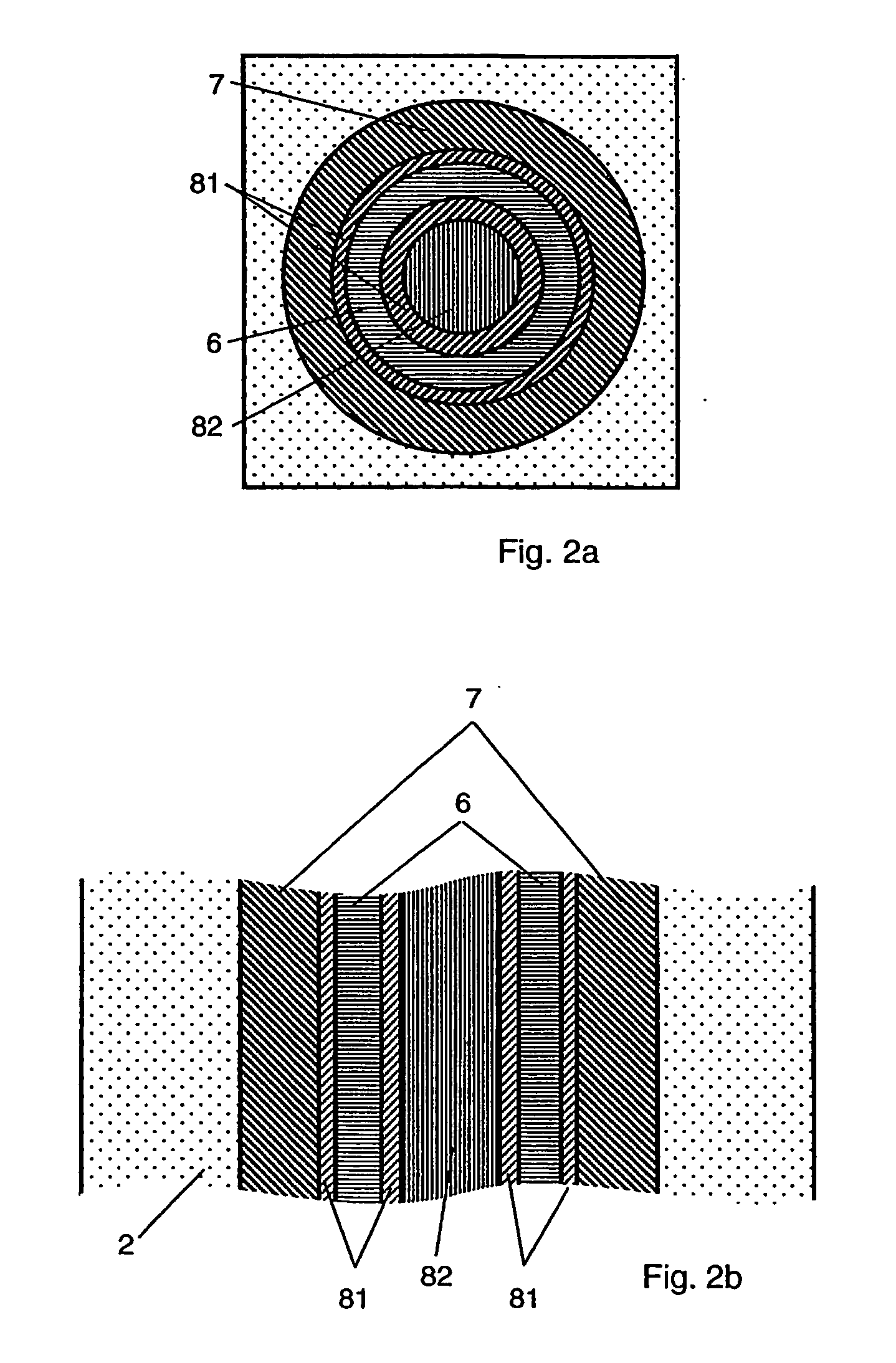
[0010] In an insulated gate semiconductor device according to the invention, a first base region of first conductivity type is disposed in a channel region of first conductivity type formed in a semiconductor substrate, so that said first base region encompasses the IGBT source regions, but does not adjoin a top surface underneath the gate insulation film. In addition, a second base region of first conductivity type is disposed in the semiconductor substrate underneath a base contact area, said base contact area being delimited by one or more source regions, so that the second base region partially overlaps the channel region and the first base region.

[0011] By laterally confining the second base region to a region under...


PUM


Abstract

In an insulated gate bipolar transistor, an improved safe operating area capability is achieved according to the invention by a two-fold base region comprising a first base region (81), which is disposed in the channel region (7) so that it encompasses the one or more source regions (6), but does not adjoin the second main surface underneath the gate oxide layer (41), and a second base region (82) is disposed in the semiconductor substrate (2) underneath the base contact area (821) so that it partially overlaps with the channel region (7) and with the first base region (81).

Description

TECHNICAL FIELD [0001] The invention relates to the field of semiconductor devices. It relates in particular to an insulated gate bipolar transistor as described in the preamble of claim 1. PRIOR ART [0002] To achieve improved safe operating area (SOA) capability in insulated gate bipolar transistors (IGBTs), a deep, highly doped p+ base region is often introduced for an increased latch-up current during device turn-off. “Deep” in this context refers to the fact that a first depth of the highly doped p+ base region is bigger than a second depth of a channel region of the IGBT. The deep p+ base region performs the following main tasks during a turn-off of the IGBT: [0003] Firstly, it efficiently collects holes during the turn-off. As a consequence, the number of holes that enter a drift region of the IGBT via a channel of the IGBT is minimized. Early parasitic thyristor latch-up is thus prevented. [0004] Secondly, by extending the p+ base region laterally, it protects n+ source regio...

Claims


Application Information

Patent Timeline
IPC IPC(8): H01L31/00H01L29/739B67D7/06B67D1/14H01L21/331H01L29/10
CPCB67D1/1422H01L29/7395H01L29/66333H01L29/1095
Inventor RAHIMO, MUNAFLINDER, STEFAN
Owner HITACHI ENERGY SWITZERLAND AG
Why Eureka
Try Eureka