Nanowire array and nanowire solar cells and methods for forming the same

a solar cell and nanowire technology, applied in the direction of final product manufacturing, sustainable manufacturing/processing, semiconductor/solid-state device details, etc., can solve the problems of high cost of manufacturing conventional solar cells, limiting their widespread use as a source of power generation, and increasing costs

Inactive Publication Date: 2007-08-23
RGT UNIV OF CALIFORNIA
View PDF4 Cites 58 Cited by
  • Summary
  • Abstract
  • Description
  • Claims
  • Application Information

AI Technical Summary

Problems solved by technology

Despite these efficiencies, the high cost of manufacturing conventional solar cells limits their widespread use as a source of power generation.
These options all result in increased costs.
Another problem with conventional solar devices is the high cost of manufacturing materials.
Because solar cells are large area devices, such material costs hinder the production of inexpensive cells.

Method used


Image

  • Nanowire array and nanowire solar cells and methods for forming the same
  • Nanowire array and nanowire solar cells and methods for forming the same
  • Nanowire array and nanowire solar cells and methods for forming the same

Examples


Embodiment Construction

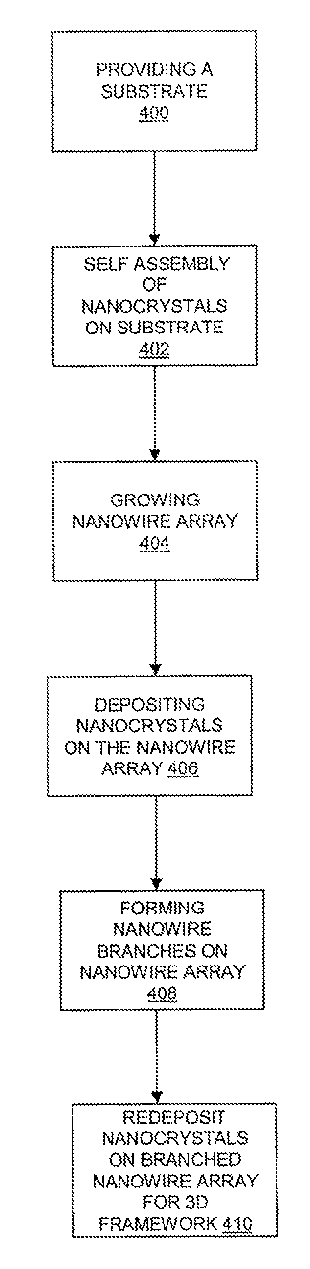
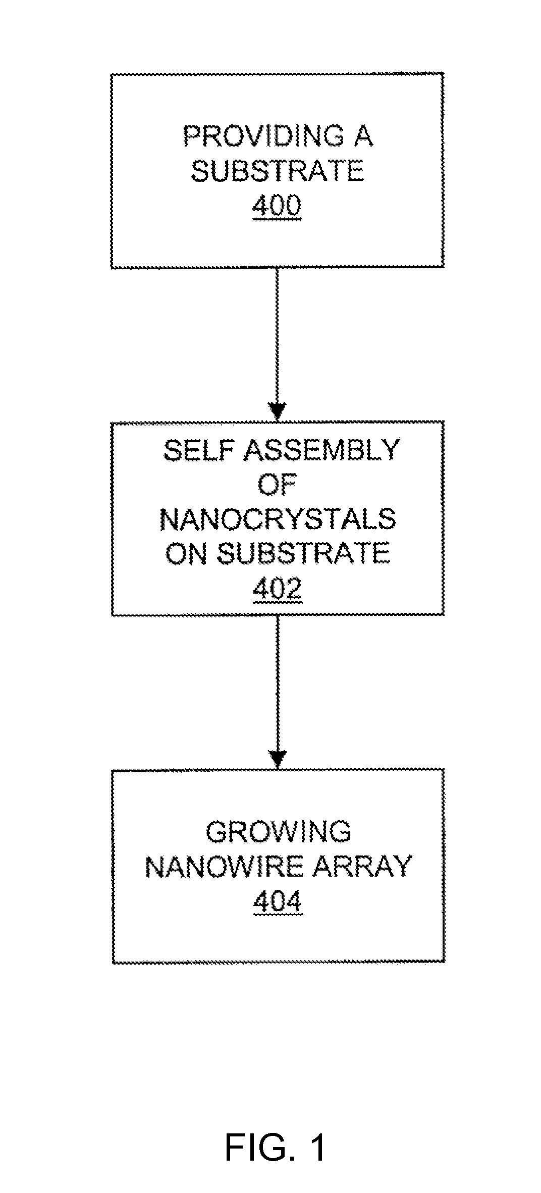
[0040] Embodiments of the invention are directed to nanowire arrays, devices including nanowire arrays, and methods for making the same. In embodiments of the invention, synthetic methods can be used to produce homogeneous and dense arrays of nanowires. The nanowires can be grown on various substrates under mild aqueous conditions. Solution approaches to producing nanowires are appealing, because they can use low temperature processing steps that are suitable for scale-up.

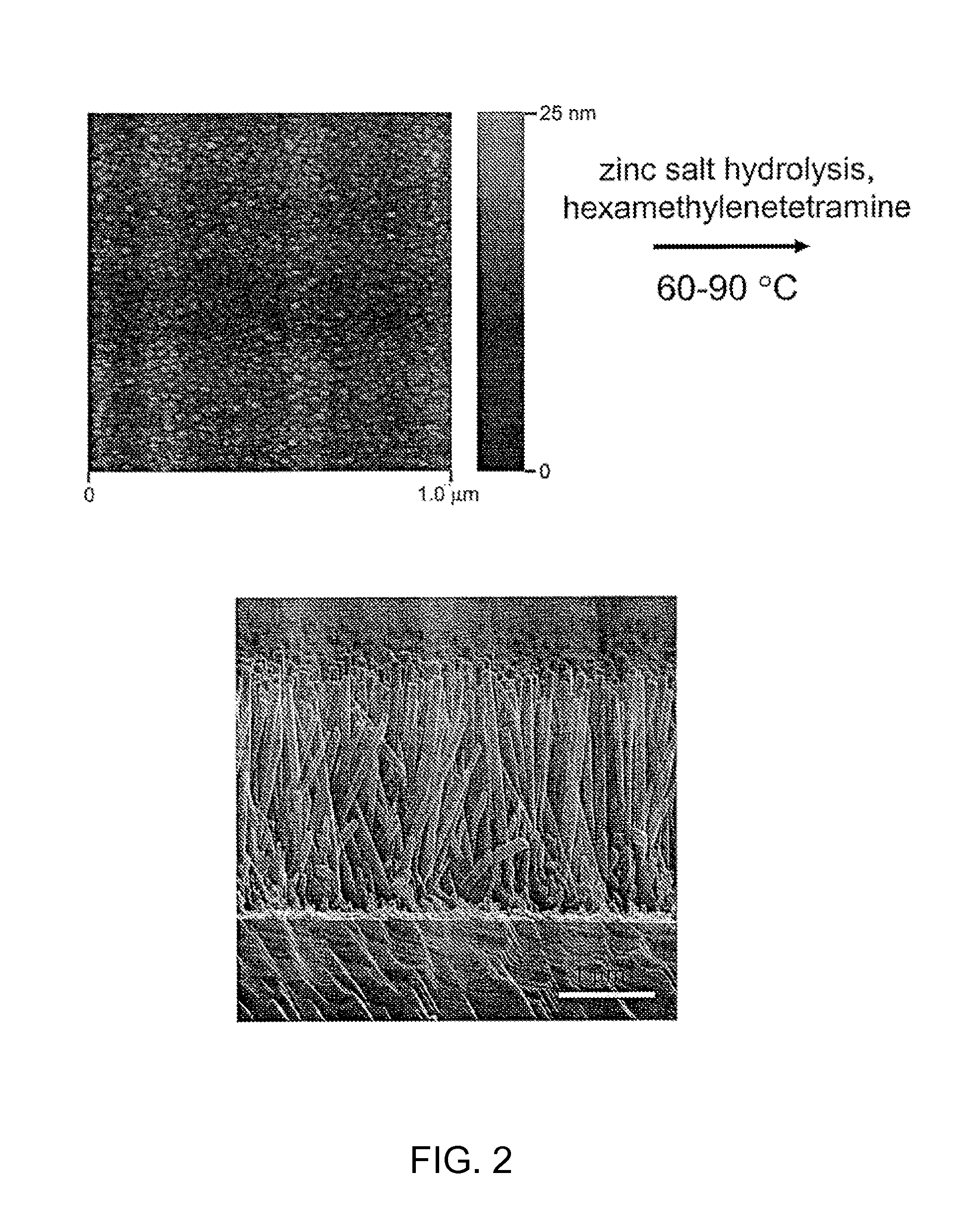
[0041] In one exemplary embodiment of the invention, homogeneous and dense arrays of ZnO nanowires were synthesized on 4-inch silicon wafers using a mild solution process at 90° C. Uniform ZnO nanocrystals were first deposited on the substrates to act as seeds for subsequent hydrothermal nanowire growth on the substrates. This procedure yielded single crystalline wurtzite ZnO nanowires grown along the [0001] direction. The nanowires were oriented perpendicular to the wafer surface. By controlling the reaction time...


PUM

PropertyMeasurementUnit
lengthsaaaaaaaaaa
lengthsaaaaaaaaaa
lengthsaaaaaaaaaa

Abstract

Homogeneous and dense arrays of nanowires are described. The nanowires can be formed in solution and can have average diameters of 40-300 nm and lengths of 1-3 μm. They can be formed on any suitable substrate. Photovoltaic devices are also described.

Description

CROSS-REFERENCES TO RELATED APPLICATIONS [0001] This patent application is a non-provisional of and claims the benefit of the filing date for U.S. Patent Application No. 60 / 480,256, filed on Jun. 20, 2003, which is herein incorporated by reference in its entirety.STATEMENT AS TO RIGHTS TO INVENTIONS MADE UNDER FEDERALLY SPONSORED RESEARCH OR DEVELOPMENT [0002] The invention described and claimed herein was made in part utilizing funds supplied by the United States Department of Energy under contract No. DE-AC03-76SF000-98 between the United States Department of Energy and The Regents of the University of California. The government has certain rights to the invention.BACKGROUND OF THE INVENTION [0003] The first solar cells were fabricated in the mid 1950s from crystalline silicon wafers. At that time, the most efficient devices converted 6% of solar power to electricity. Advancements in solar cell technology over the past 50 years have resulted in the most efficient Si cell being at ...

Claims


Application Information

Patent Timeline
Patent Type & Authority Applications(United States)
IPC IPC(8): H01L21/00H01G9/20H01L51/00H01L51/30
CPCB82Y30/00H01G9/2027H01L2924/0002H01L21/0237H01L21/02554H01L21/02603H01L21/02628H01L21/02639H01L33/08H01L33/20H01L51/0036H01L51/0038H01L51/0086H01L51/4233Y02E10/542Y10S977/811Y10S977/762Y02E10/549H01L2924/00Y02P70/50H10K85/113H10K85/114H10K85/344H10K30/152
Inventor YANG, PEIDONGGREENE, LORI E.LAW, MATTHEW
Owner RGT UNIV OF CALIFORNIA
Why Eureka
Try Eureka