
Methods for tiling integrated circuit designs

a technology of integrated circuits and design methods, applied in the field of integrated circuit design, can solve the problems of extremely high computational resources and the inability to realize the full potential of computational resources, and achieve the effect of reducing the potential of computational resources and reducing the complexity of the design process

Inactive Publication Date: 2007-08-23
ATHENA DESIGN SYST
View PDF51 Cites 5 Cited by
  • Summary
  • Abstract
  • Description
  • Claims
  • Application Information

AI Technical Summary

Problems solved by technology

However, due to the ever-increasing electrical constraints, modern ICs bound all routing geometries to metal layers, wherever such layers have not been utilized by the connections within the library modules or IP building blocks.
Due to the fact that a typical IC consists of millions of nets, a routing of a single net is a NP-hard problem.
This fact indicates a potential of extremely high demands on computational resources.

Method used


Image

  • Methods for tiling integrated circuit designs
  • Methods for tiling integrated circuit designs
  • Methods for tiling integrated circuit designs

Examples


Embodiment Construction

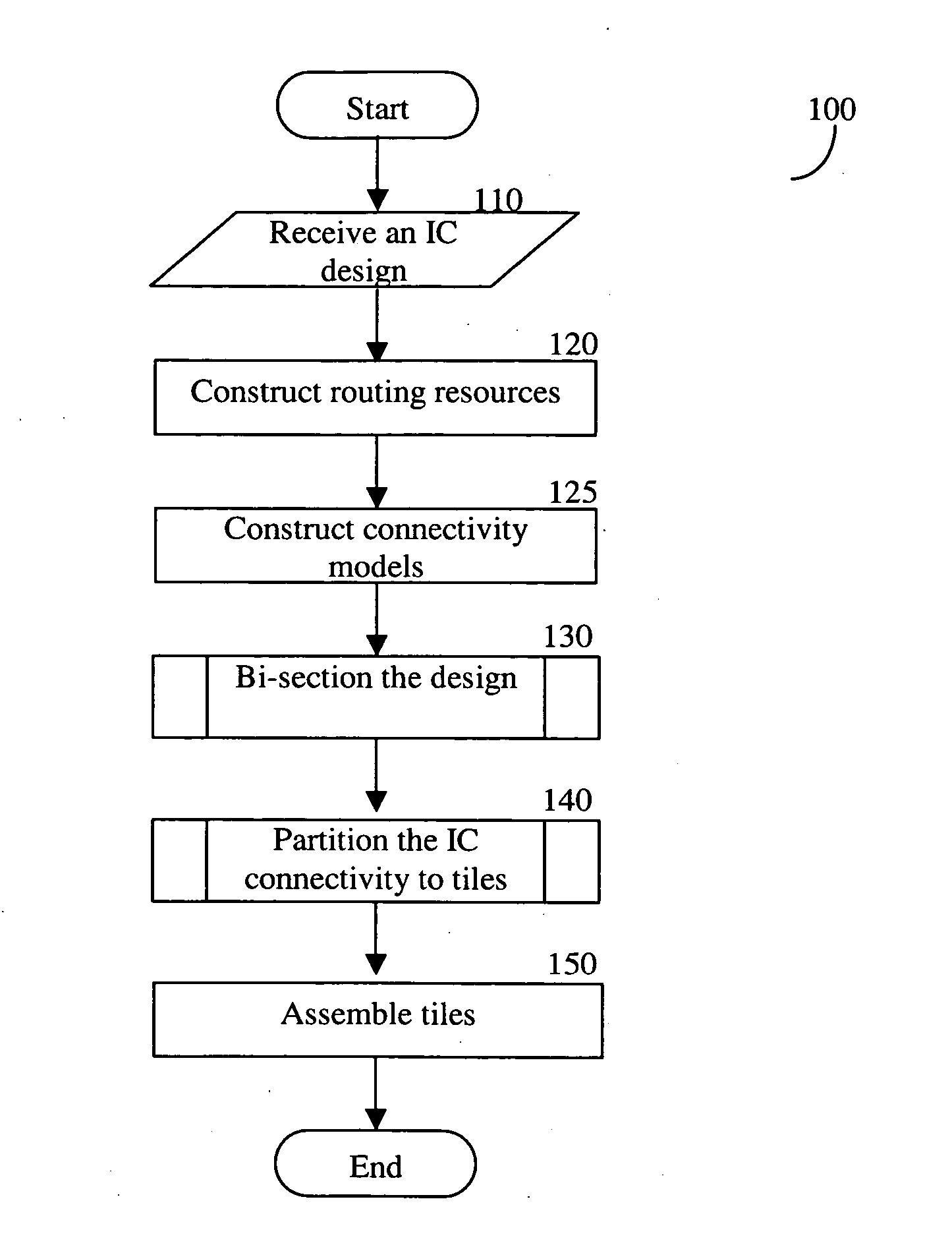
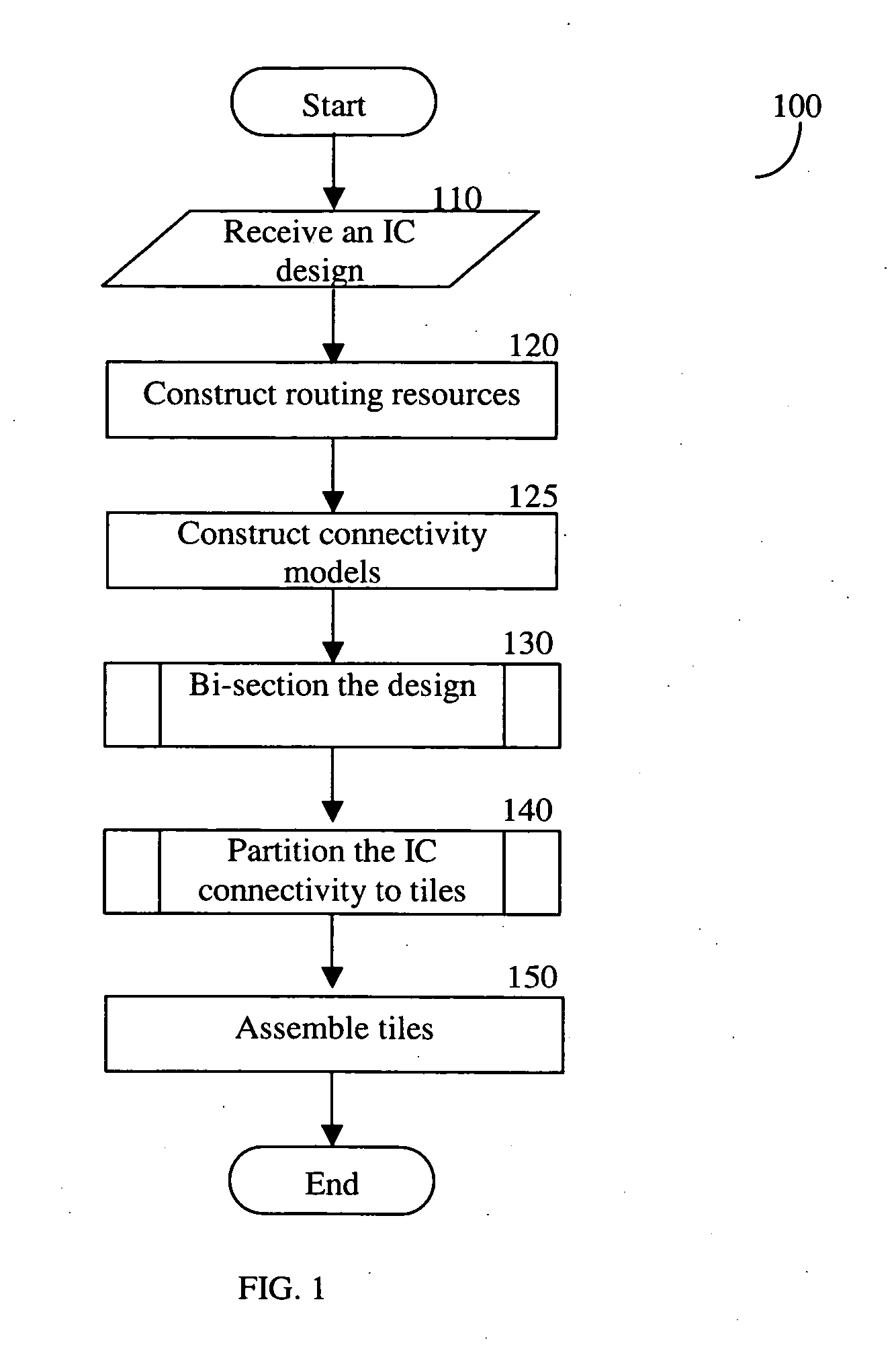
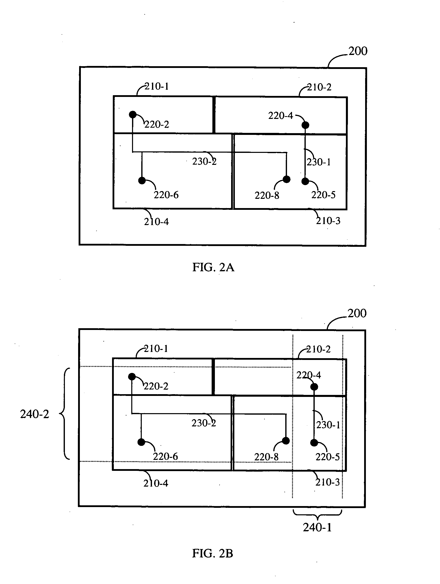
[0016] The present invention comprises a method that allows the simplification of the routing phase in the design of integrated circuits (ICs). Using the disclosed method, the time expended on the routing task is significantly reduced. The method includes dividing a given IC design into a limited number of non-overlapping tiles, and then routing all tiles in parallel, each tile being independently routed by a standard router. Thereafter, routed tiles are assembled to form a routing solution for the entire IC.

[0017]FIG. 1 shows an exemplary and non-limiting flowchart 100 describing a method for tiling an IC design in accordance with one embodiment of the present invention. At 110, the files of an IC design to be tiled are received. The input design may be a result of a placement or routing tool. Input from a global router can be utilized to tile the design and then routing the tiles using fine routers. Input from a fine router can be utilized for tiling the design for the purpose of...


PUM


Abstract

Methods for routing in the design of integrated circuits (ICs) to simplify the routing task. The method includes dividing a given IC design into a limited number of non-overlapping tiles, and then routing all tiles in parallel, each tile being independently routed by a standard router. Thereafter, routed tiles are assembled to form a routing solution for the entire IC. Details of exemplary methods are disclosed.

Description

BACKGROUND OF THE INVENTION [0001] 1. Field of the Invention [0002] The present invention relates generally to the design of integrated circuits (ICs), and more particularly to the routing phase of an IC design. [0003] 2. Prior Art [0004] Due to the ever increasing complexity of integrated circuit (IC) designs, IC designers become more and more reliant on electronic design automation (EDA) tools. An IC is fabricated by a series of lithographic steps that may be abstracted as a construction of a multilayered stack of materials, each layer consisting of a large set of simple geometries. In the related art, EDA tools that manipulate modular sets (e.g., component libraries, IP blocks, and so on) of simple geometries are provided. Each such modular set consists of geometries that exist on several or all lithographic layers of the IC and contains a logic function, ranging from a simple inverter library cell to an IP block module that may hold a microprocessor. [0005] Generally, the proces...

Claims


Application Information

Patent Timeline
Patent Type & Authority Applications(United States)
IPC IPC(8): G06F17/50G06F9/45
CPCG06F17/5077G06F17/5068G06F30/39G06F30/394G06F30/3947
Inventor FOTAKIS, DIMITRIS K.JUKL, MILAN F.
Owner ATHENA DESIGN SYST
Learn More