

Memory transistor gate oxide stress release and improved reliability
a technology of memory transistors and gate oxides, applied in the field of memory cells, can solve problems such as soft or hard breakdown, several detrimental physical effects, and beginning to show fundamental limits associated with quantum mechanics and fabrication techniques limitations
Active Publication Date: 2007-09-06
SYNOPSYS INC
View PDF4 Cites 2 Cited by
- Summary
- Abstract
- Description
- Claims
- Application Information
AI Technical Summary
Problems solved by technology
The MOS (Metal-Oxide-Semiconductor) devices, which are the current basis of Ultra-Large-Scale Integration circuits such as memory circuits, are beginning to show fundamental limits associated with the laws of quantum mechanics and the limitations of fabrication techn
Method used
View moreImage
Smart ImageViewing Examples

Examples
 PUM
 Abstract
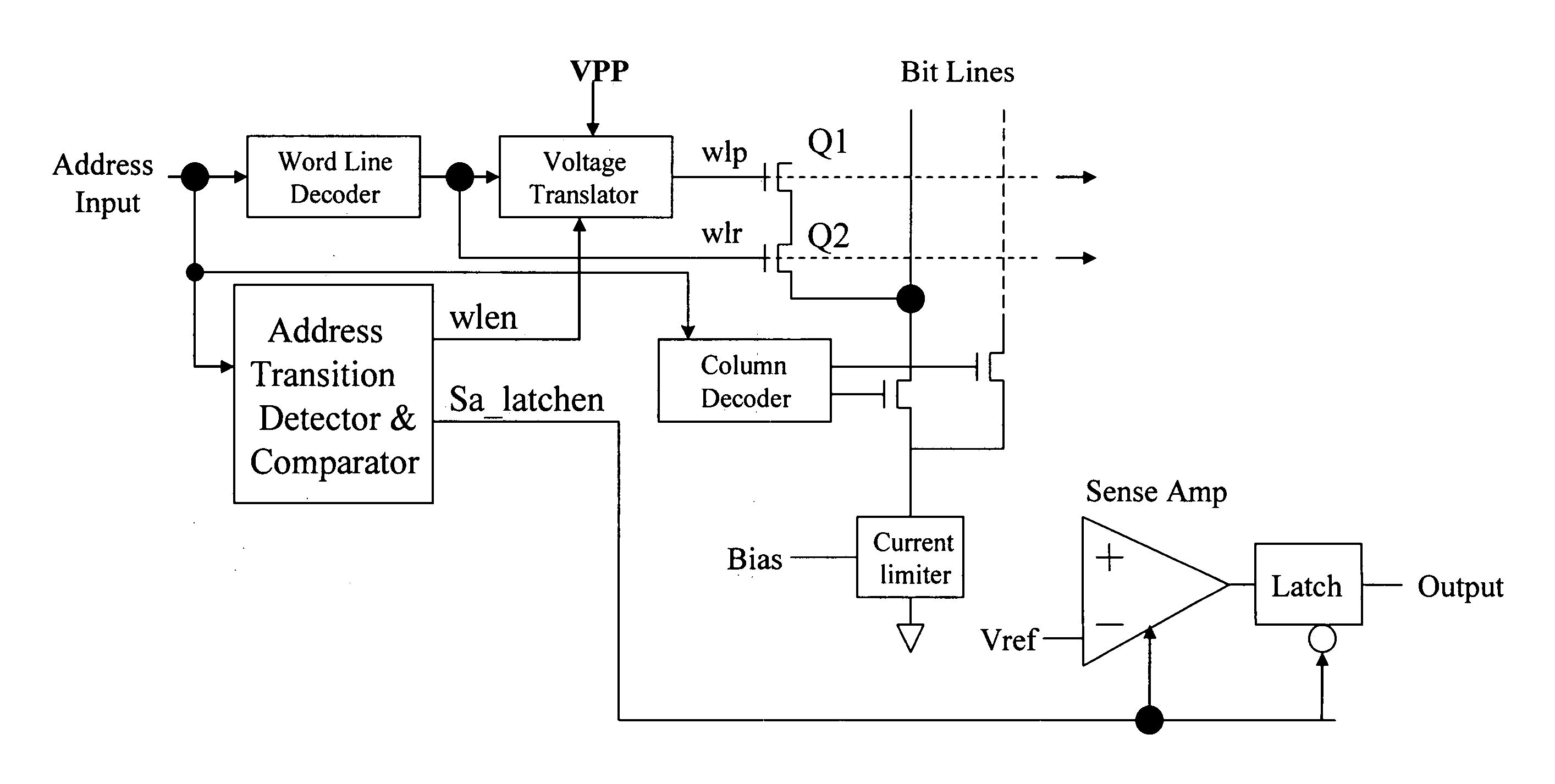
Methods and apparatus for decreasing oxide stress and increasing reliability of memory transistors are disclosed. Duration and frequency of exposure of memory transistor gates to read signals are significantly reduced. In some embodiments, after a short read cycle, the content of the memory cell is latched and maintained as long as the subsequent read attempts are directed to the same memory cell. In these embodiments the read cycle need only be long enough to latch the memory content of the cell, and as long as the subsequent read attempts target the same memory cell the latched value will be used instead of repeating the read process.
Description
TECHNICAL FIELD OF THE INVENTION [0001] The presented embodiments relate, in general, to memory cells and, more particularly, to reducing stress on memory devices. BACKGROUND OF THE INVENTION [0002] Nonvolatile memory circuits have been widely used in various circuit applications including computer memory, automotive applications, FPGAs (field programmable gate arrays), communication equipment, video games, code storage memories, serial configuration memories, and individual fuse bits for ID, trimming, and other post-fab SoC customization needs. The MOS (Metal-Oxide-Semiconductor) devices, which are the current basis of Ultra-Large-Scale Integration circuits such as memory circuits, are beginning to show fundamental limits associated with the laws of quantum mechanics and the limitations of fabrication techniques. [0003] In MOS structures, the gate insulator, which is formed by an oxide layer, endures high electric fields during operation. This stress causes several detrimental phys...
Claims
Login to View More Application Information
Patent Timeline
 IPC IPC(8): G11C16/06G11C11/34
CPCG11C7/08G11C7/18G11C2207/065G11C2207/061G11C16/28
InventorFONG, DAVIDWANG, JIANGUOPENG, JACK Z.LUAN, HARRY S.
OwnerSYNOPSYS INC