Integrated circuit package system with post-passivation interconnection and integration

a post-passivation interconnection and integrated circuit technology, applied in the field of integrated circuits, can solve the problems large size of analog circuit components, and difficulty in integrating into integrated circuits, and achieve the effects of reducing the difficulty of conventional gold wire bonding technology, avoiding the occurrence of bare copper pads, and avoiding bare copper pads

Inactive Publication Date: 2007-10-11
STATS CHIPPAC LTD
View PDF6 Cites 37 Cited by
  • Summary
  • Abstract
  • Description
  • Claims
  • Application Information

AI Technical Summary

Problems solved by technology

One of the major challenges in the creation of analog processing circuitry (using digital processing procedures and equipment) is that a number of the components that are used for analog circuitry are large in size and are therefore not readily integrated into integrated circuits.
The main components that offer a challenge in this respect are capacitors and inductors, since both these components are, f

Method used


Image

  • Integrated circuit package system with post-passivation interconnection and integration
  • Integrated circuit package system with post-passivation interconnection and integration
  • Integrated circuit package system with post-passivation interconnection and integration

Examples


Embodiment Construction

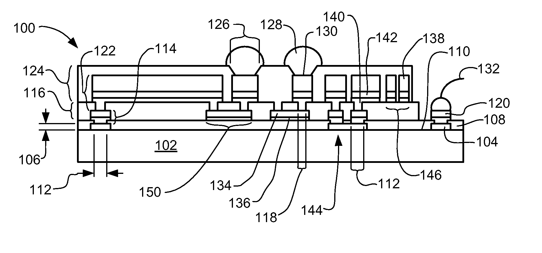
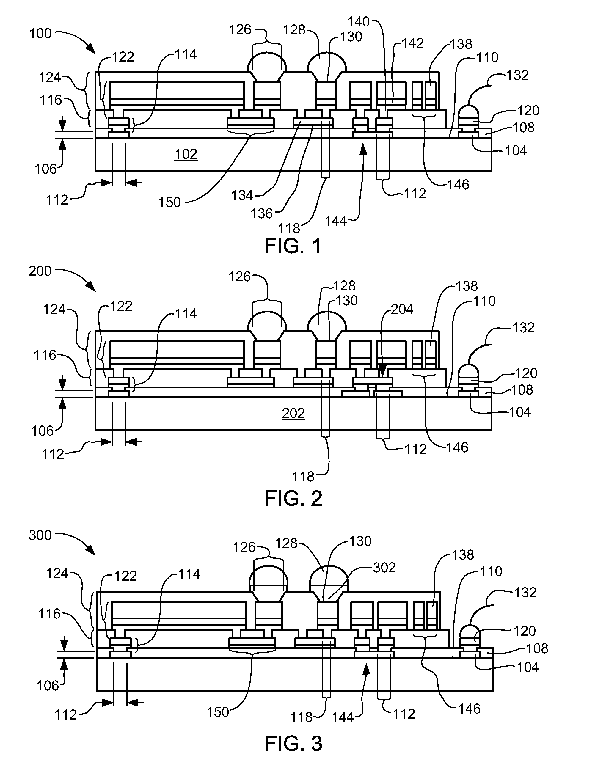
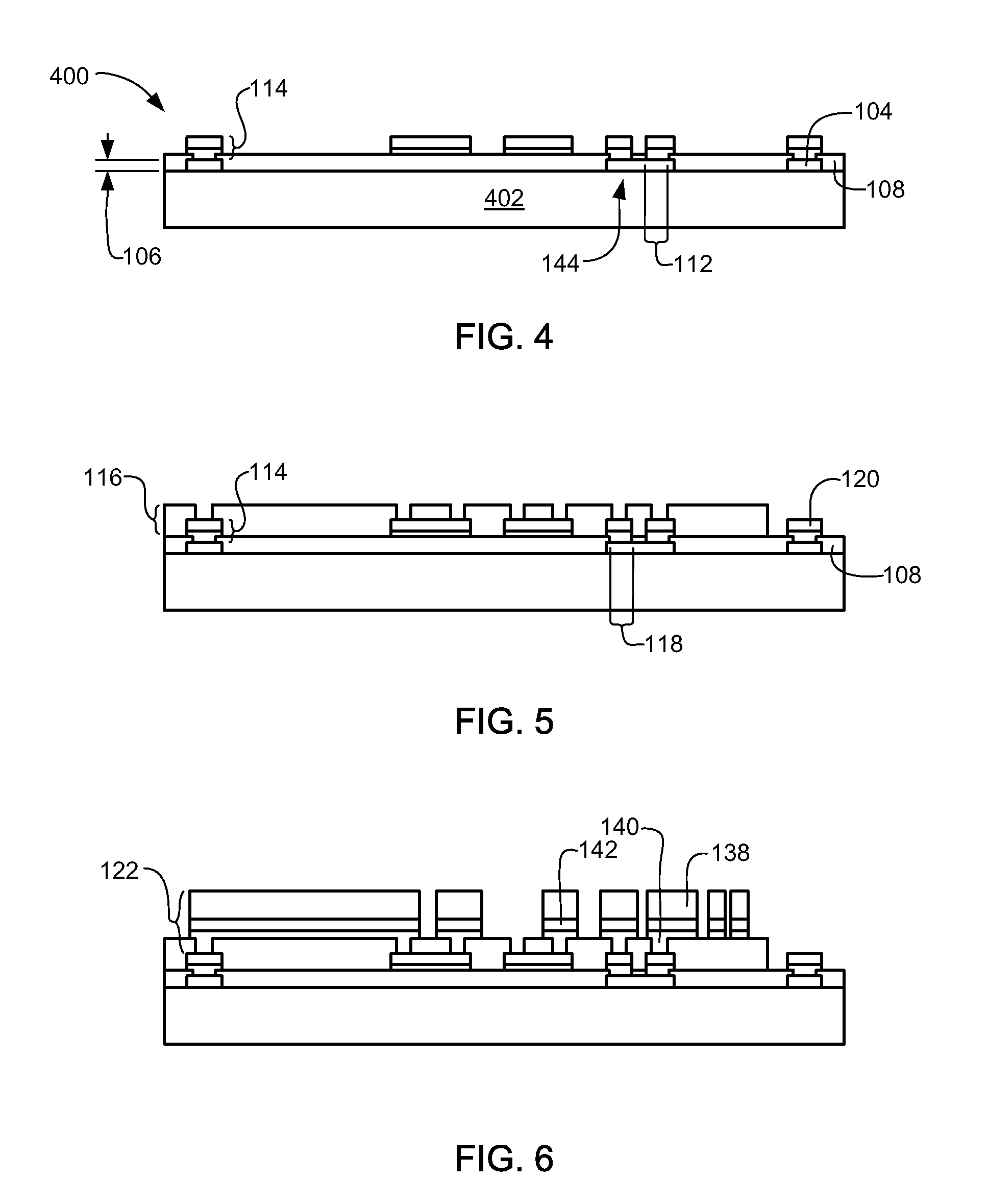
[0018] In the following description, numerous specific details are given to provide a thorough understanding of the invention. However, it will be apparent that the invention may be practiced without these specific details. In order to avoid obscuring the present invention, some well-known system configurations, and process steps are not disclosed in detail. Likewise, the drawings showing embodiments of the apparatus are semi-diagrammatic and not to scale and, particularly, some of the dimensions are for the clarity of presentation and are shown greatly exaggerated in the figures. The same numbers are used in all the figures to relate to the same elements.

[0019] The term “horizontal” as used herein is defined as a plane parallel to the conventional integrated circuit surface, regardless of its orientation. The term “vertical” refers to a direction perpendicular to the horizontal as just defined. Terms, such as “above”, “below”, “bottom”, “top”, “side” (as in “sidewall”), “higher”, ...


PUM


Abstract

An integrated circuit package system is provided providing an integrated circuit die having a final metal layer of the semiconductor process used to manufacture the integrated circuit die and a passivation layer provided thereon, depositing a first metal layer on the passivation layer and the final metal layer, forming an analog circuit in the first metal layer, coating a first insulation layer on the first metal layer and the passivation layer, exposing a first pad and a second pad of the first metal layer through the first insulation layer, and connecting a first interconnect on the first pad and a second interconnect on the second pad.

Description

TECHNICAL FIELD [0001] The present invention relates generally to integrated circuits and more particularly to integrated circuit packaging. BACKGROUND ART [0002] Modern consumer electronics, such as smart phones, personal digital assistants, and location based services devices, as well as enterprise electronics, such as servers and storage arrays, are packing more integrated circuits into an ever shrinking physical space with expectations for decreasing cost. Every new generation of integrated circuits with increased operating frequency, performance and the higher level of large scale integration have underscored the need for back-end semiconductor manufacturing to provide more solutions involving the integrated circuit itself. Numerous technologies have been developed to meet these requirements. Some of the research and development strategies focus on new package technologies while others focus on improving the existing and mature package technologies. Both approaches may include ...

Claims


Application Information

Patent Timeline
IPC IPC(8): H01L23/48
CPCH01L23/5227H01L2224/0401H01L23/53223H01L23/53238H01L24/05H01L24/13H01L2224/48463H01L2224/13022H01L2224/45144H01L23/525H01L2224/04042H01L2224/0554H01L2224/05001H01L2924/00H01L2924/14
Inventor LIN, YAOJIANMARIMUTHU, PANDI CHELVAM
Owner STATS CHIPPAC LTD
Why Eureka
Try Eureka