Varied impurity profile region formation for varying breakdown voltage of devices

a technology of impurity profile and device, applied in the field of forming a varied impurity profile region, can solve the problems of unsatisfactory approaches, disadvantageous doping of the exposed silicon closest to the edge of the resist, and high implementation costs of bipolar technologies

Inactive Publication Date: 2007-11-29
GLOBALFOUNDRIES INC
View PDF23 Cites 0 Cited by
  • Summary
  • Abstract
  • Description
  • Claims
  • Application Information

AI Technical Summary

Problems solved by technology

As a result of the additional mask / implant steps, bipolar technologies are expensive to implement.
However, these approaches are unsatisfactory because the thick resist needed to block the deep N-Well implants compromises the ground rules needed to minimize the size of the NPN device.
These scattered ions may disadvantageously dope the surface of the exposed silicon closest to the edge of the resist.

Method used


Image

  • Varied impurity profile region formation for varying breakdown voltage of devices
  • Varied impurity profile region formation for varying breakdown voltage of devices
  • Varied impurity profile region formation for varying breakdown voltage of devices

Examples


Embodiment Construction

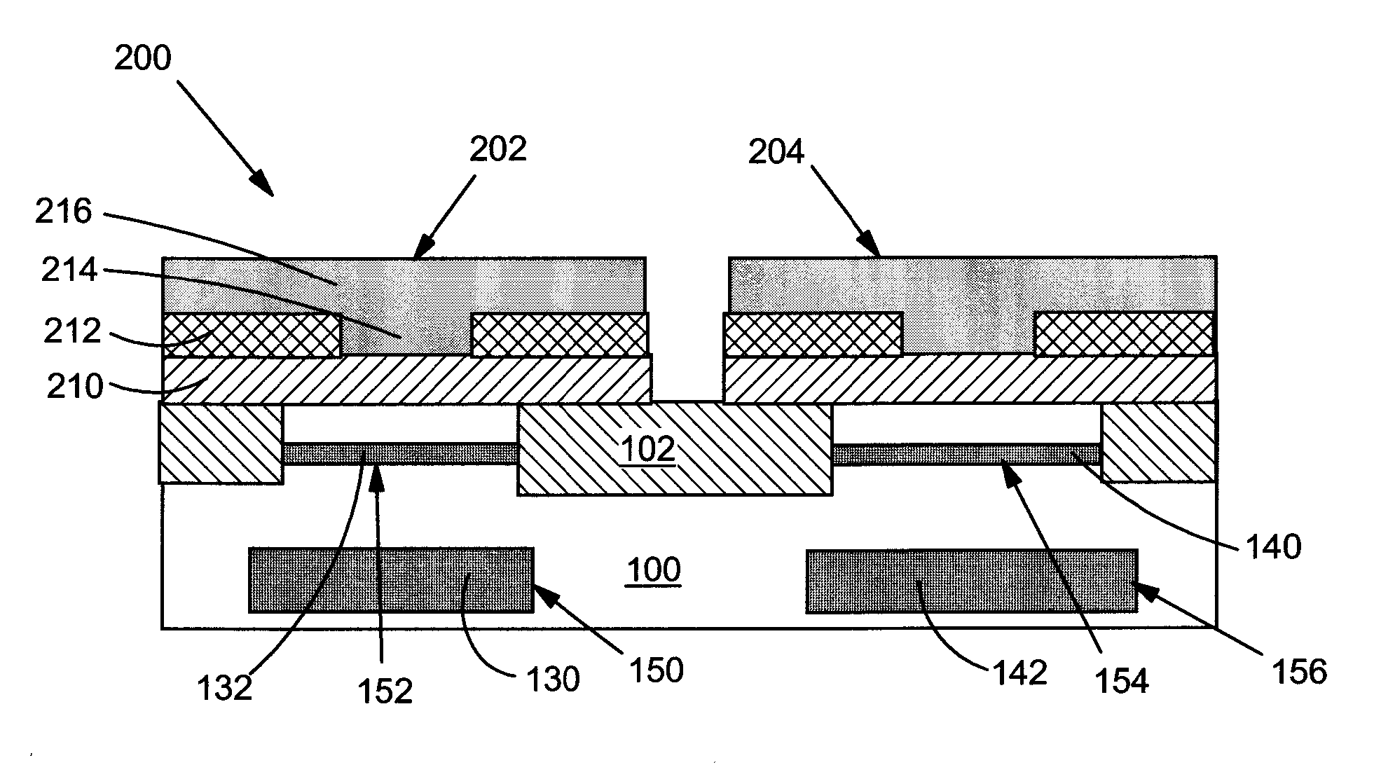
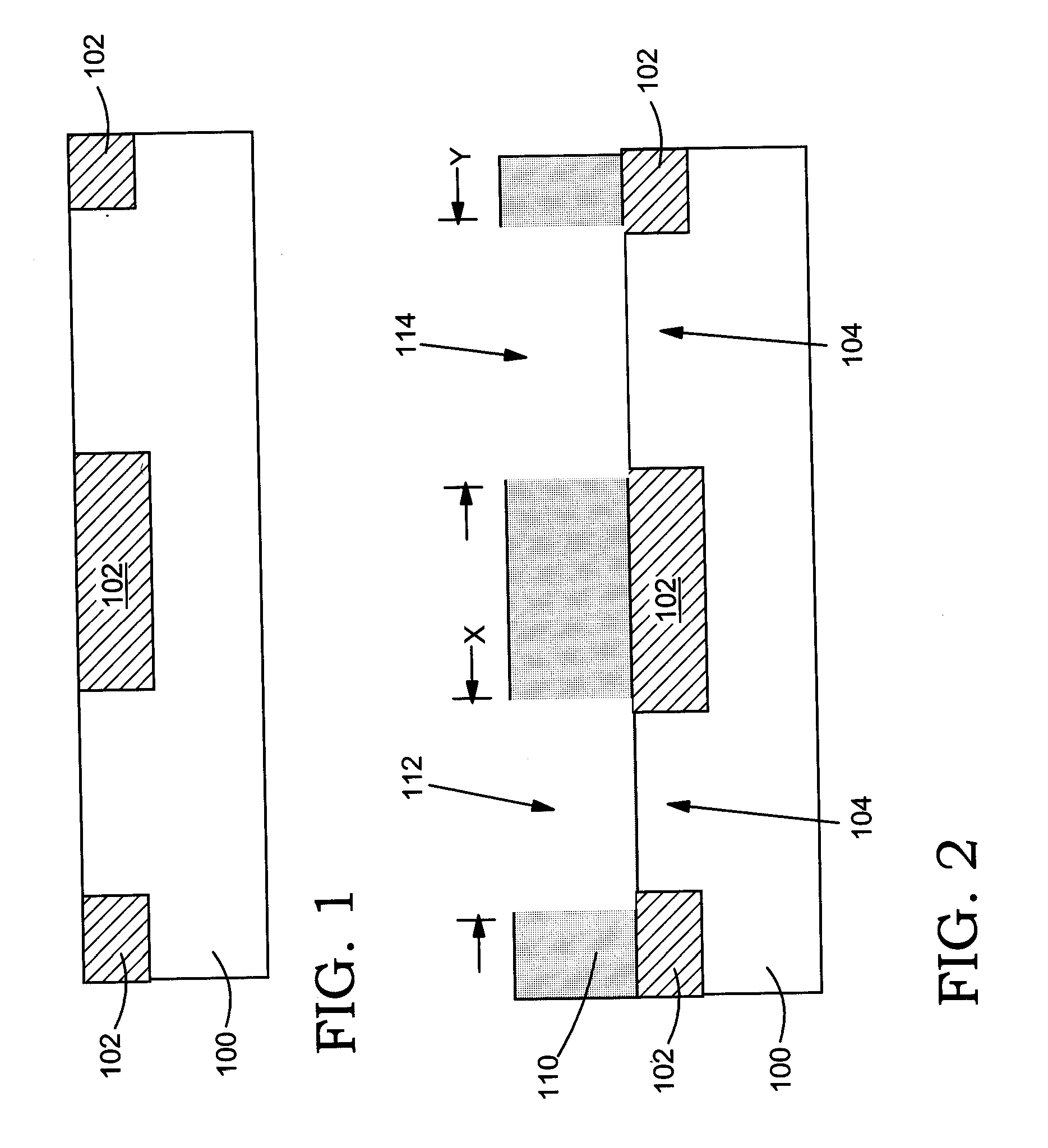
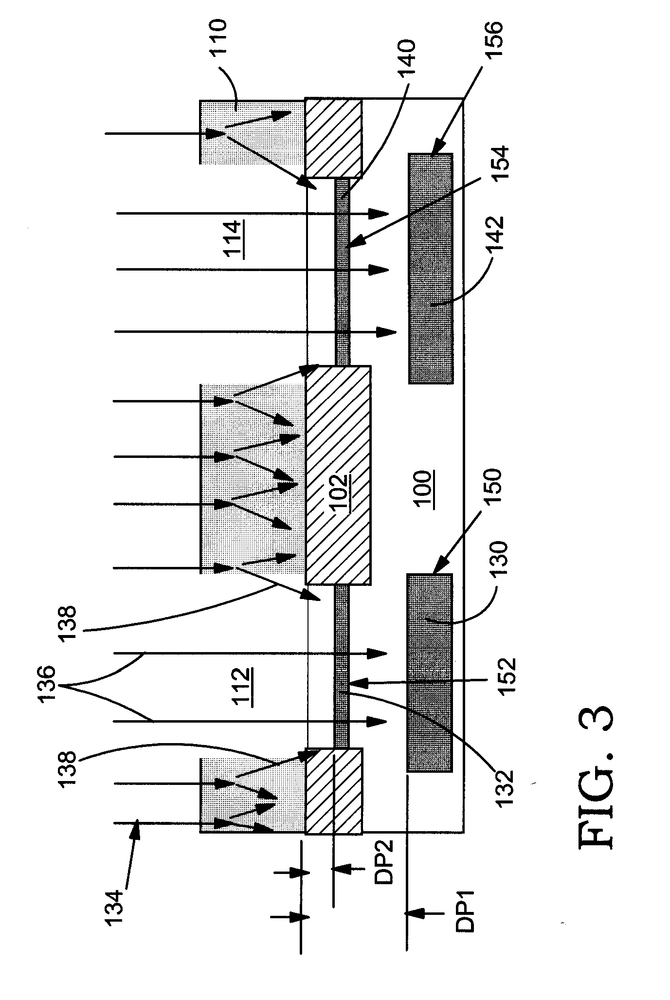
[0020] With reference to the accompanying drawings, FIGS. 1-3 show a method according to one embodiment of the invention. In one embodiment, the invention includes providing a substrate 100, e.g., of silicon, including a number of shallow trench isolations (STI) 102 surrounding selected active regions 104 (FIG. 2) for bipolar transistors to be formed.

[0021] Next, as shown in FIG. 2, a mask layer 110 is formed on substrate 100 including a first opening 112 having a first dimension X. Mask layer 110 may include any now known or later developed resist mask material. Alternatively, mask layer 110 may include a hard mask material (e.g., silicon dioxide (SiO2)) instead of a resist mask to avoid possible manufacturing control problems, although this is more expensive and not the preferred method. In addition to first opening 112, any number of second openings 114 may also be formed for any number of devices (not shown) to be formed on substrate 100. A second opening 114 has a second dimen...


PUM


Abstract

Methods are disclosed for forming a varied impurity profile for a collector using scattered ions while simultaneously forming a subcollector. In one embodiment, the invention includes: providing a substrate; forming a mask layer on the substrate including a first opening having a first dimension; and substantially simultaneously forming through the first opening a first impurity region at a first depth in the substrate (subcollector) and a second impurity region at a second depth different than the first depth in the substrate. The breakdown voltage of a device can be controlled by the size of the first dimension, i.e., the distance of first opening to an active region of the device. Numerous different sized openings can be used to provide devices with different breakdown voltages using a single mask and single implant. A semiconductor device is also disclosed.

Description

CROSS-REFERENCE TO RELATED APPLICATIONS [0001] This application is a Divisional Application of co-pending U.S. patent application Ser. No. 10 / 908,884, filed May 31, 2005.BACKGROUND OF THE INVENTION [0002] 1. Technical Field [0003] The present invention relates generally to semiconductor devices, and more particularly, to forming a varied impurity profile region for varying breakdown voltages of different devices. [0004] 2. Related Art [0005] Bipolar semiconductor device technologies typically require multiple devices having different breakdown voltages on the same wafer for various circuit applications. Devices with different breakdown voltages have different performances due to the change in the collector transit time of the device that is obtained by varying the collector impurity profile between devices, which also modulates the breakdown voltage. [0006] Multiple breakdown voltage devices are typically obtained by using a different mask and implant to tailor the collector impurit...

Claims


Application Information

Patent Timeline
Patent Type & Authority Applications(United States)
IPC IPC(8): H01L21/331
CPCH01L21/266H01L21/8222H01L29/36H01L29/0821H01L27/0825
Inventor COOLBAUGH, DOUGLAS D.LANZEROTTI, LOUIS D.ORNER, BRADLEY A.RASCOE, JAY S.SHERIDAN, DAVID C.ST. ONGE, STEPHEN A.
Owner GLOBALFOUNDRIES INC
Why Eureka
Try Eureka