Chip stack with a higher power chip on the outside of the stack

a technology of chip stack and power chip, which is applied in the direction of digital storage, semiconductor/solid-state device details, instruments, etc., can solve the problems of chip performance decline, chip malfunction,

Inactive Publication Date: 2007-12-20
INTEL CORP
View PDF16 Cites 63 Cited by
  • Summary
  • Abstract
  • Description
  • Claims
  • Application Information

AI Technical Summary

Problems solved by technology

If the temperature becomes too high, the chips may malfunction.
However, with a lower frequency and voltage, the performance of the chip can also decrease.

Method used


Image

  • Chip stack with a higher power chip on the outside of the stack
  • Chip stack with a higher power chip on the outside of the stack
  • Chip stack with a higher power chip on the outside of the stack

Examples


Embodiment Construction

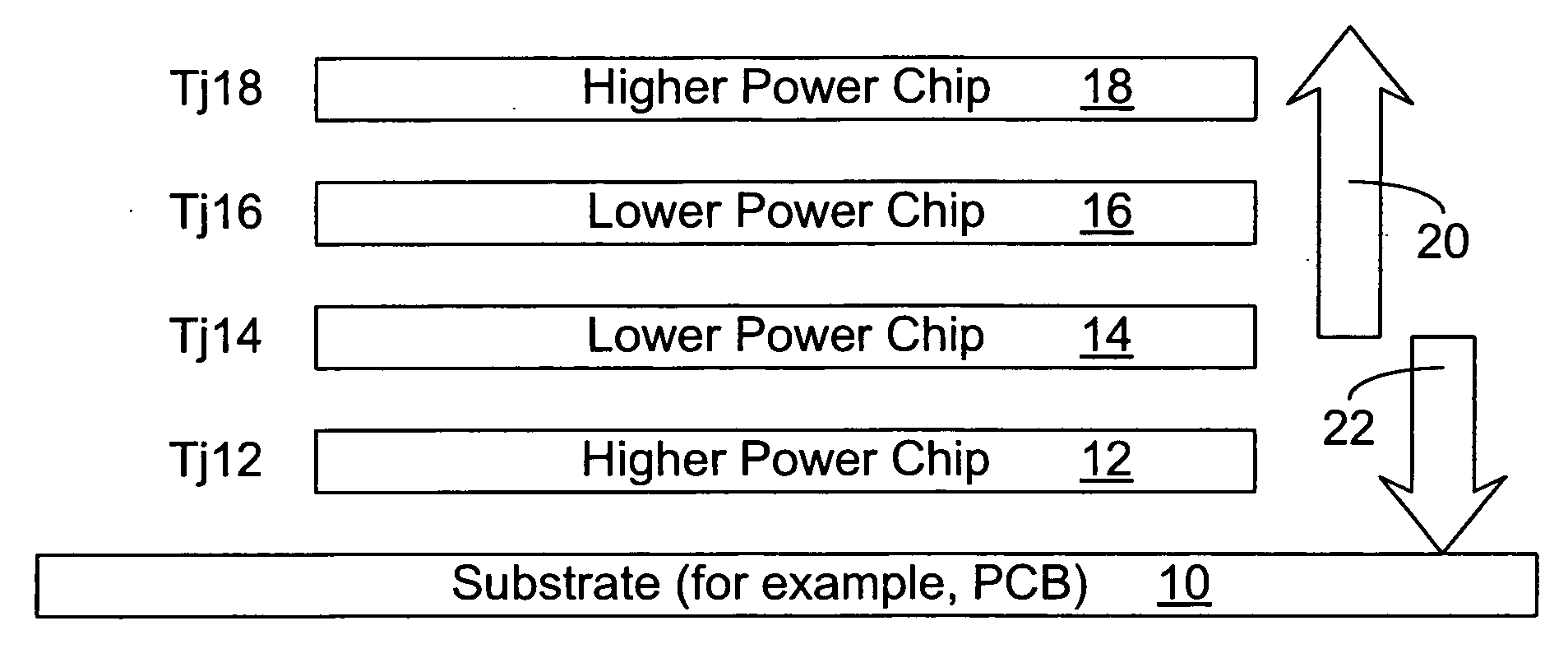
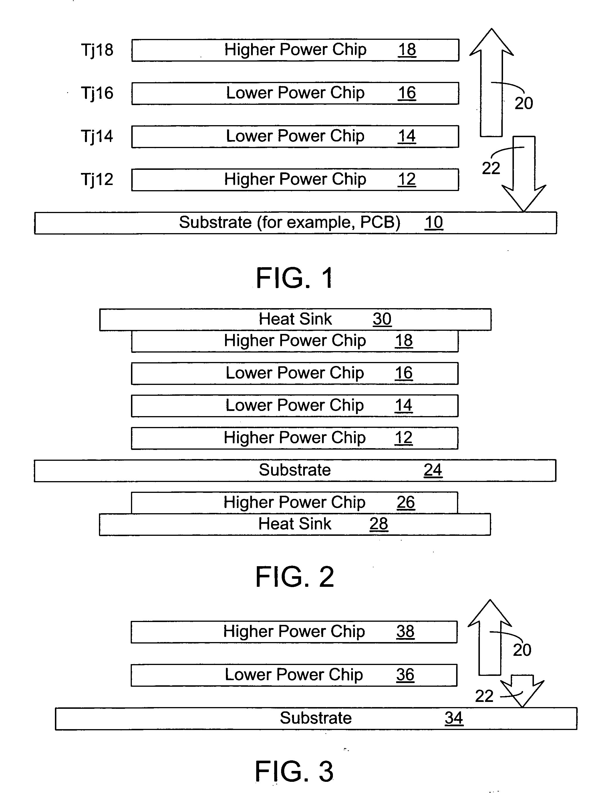
[0018]FIG. 1 illustrates a schematic representation of a system including a substrate 10 that supports a stack of chips 12, 14, 16, and 18. For clarity, spaces are shown between chips and between chip 12 and substrate 10, but in actual implementations there would be some structure between them or they would be next to each other. Chips 12-18 could be packaged. Substrate 10 may be, for example, a printed circuit board (PCB), but that is not required. In some embodiments, substrate 10 is a motherboard, which supports a variety of other components. In other embodiments, substrate 10 is a card substrate (such as a memory module substrate or graphics card substrate) that is in turn supported by a motherboard. Arrows 20 and 22 show major directions of heat flow (but certainly not the only directions of heat flow). As can be seen, in the example of FIG. 1, chips 16 and 18 have heat dissipation primarily in the direction of arrow 20. Chip 14 has heat dissipation in the directions of both ar...


PUM


Abstract

In some embodiments, a system includes a circuit board, a first chip, and a second chip stacked on the first chip. The first chip is coupled between the circuit board and the second chip, and the first chip includes circuitry to repeats commands the first chip receives to the second chip. Other embodiments are described.

Description

BACKGROUND[0001]1. Technical Field[0002]Chip stacks are described in which higher power chips are positioned in locations with greater heat dissipation abilities.[0003]2. Background Art[0004]Various arrangements for memory chips in a memory system have been proposed. For example, in a traditional synchronous dynamic random access memory (DRAM) system, memory chips communicate data through multi-drop bidirectional data buses and receive commands and addresses through command and addresses buses. More recently, bidirectional or unidirectional point-to-point interconnects have been proposed.[0005]In some systems, chips (also called dies) are stacked one on top of another. The chips may be all of the same type or some of the chips may be different than others. For example, a stack of memory chips (e.g., flash or DRAM) may be supported by a module substrate. A stack may include a chip with a memory controller. A stack may include a processor chip (with or without a memory controller) and...

Claims


Application Information

Patent Timeline
Patent Type & Authority Applications(United States)
IPC IPC(8): H01L23/34
CPCG11C5/02G11C5/063H01L25/0657H01L2924/0102H01L2224/4824H01L2225/06572H01L2225/06589H01L25/18G11C11/40H01L23/12
Inventor SAINI, MANISHMEHTA, DEEPA S.
Owner INTEL CORP
Why Eureka
Try Eureka