

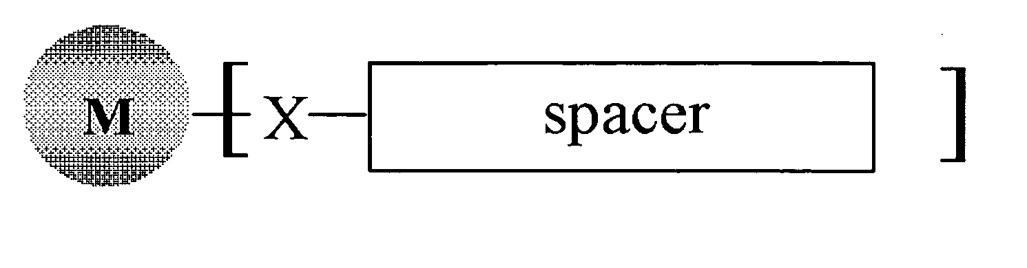
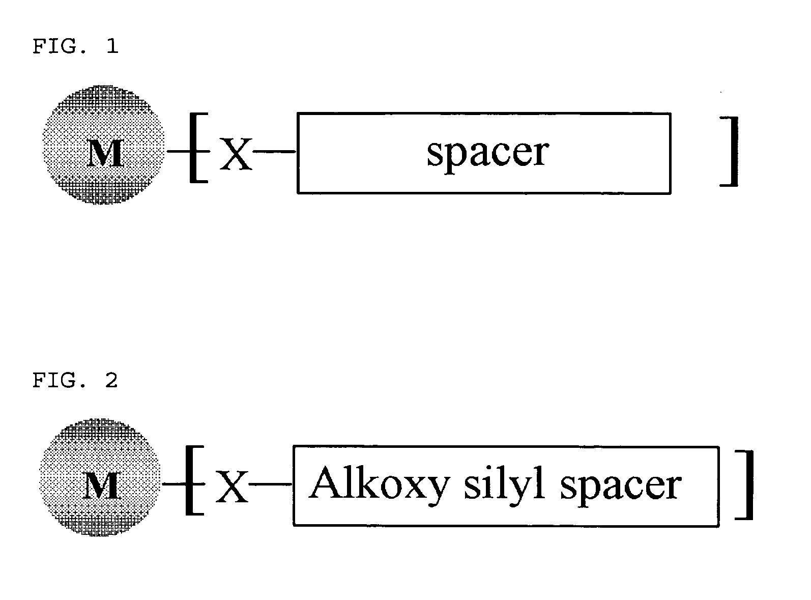
Novel metal nanoparticle and method for formation of conductive pattern using the same
a metal nanoparticle and conductive pattern technology, applied in the direction of superimposed coating process, liquid/solution decomposition chemical coating, manufacturing tools, etc., can solve the problems of difficult preparation of large-area films, limiting commercial applications, and difficulty in placing metal nanoparticles into films or patterns, etc., to achieve the effect of easy arrangement of metal nanoparticles over a large area
- Summary
- Abstract
- Description
- Claims
- Application Information
AI Technical Summary
Benefits of technology
Problems solved by technology
Method used
Image

Examples
example 1
Introduction of Organic Group into Surface of Gold Nanoparticles
[0058]0.2 g of the gold nanoparticles prepared in Preparative Example 1 was dispersed in 50 ml of 1:1 mixture of concentrated sulfuric acid and 30% hydrogen peroxide, and were slowly stirred for 20 minutes. Then, the dispersion was diluted with 250 ml of distilled water, filtered through a 0.2 μm filter, washed 5 times with 50 ml of methanol and then dried in an oven at 160° C. for 5 hours. 0.1 g of the thus-dried gold nanoparticles was added in combination with 1.3 g of 4-cyanophenol to 200 ml of toluene and the mixture was stirred for 72 hours. The resulting products were filtered through a 0.2 μm filter, washed twice with THF, and were then dried in an oven at 30° C. under reduced pressure, thereby obtaining gold nanoparticles having hydroxyl moieties connected via an isocyanide group on the surface thereof.
example 2
Introduction of Organic Group into Surface of Silver Nanoparticles
[0059]Silver nanoparticles having hydroxyl moieties connected via an isocyanide group on the surface thereof were obtained in the same manner as in Example 1, except that 0.2 g of the silver nanoparticles prepared in Preparative Example 2 was used instead of the gold nanoparticles.
example 3
Introduction of Organic Group into Surface of Copper Nanoparticles
[0060]Copper nanoparticles having hydroxyl moieties connected via an isocyanide group on the surface thereof were obtained in the same manner as in Example 1, except that 0.2 g of the copper nanoparticles prepared in Preparative Example 3 was used, instead of the gold nanoparticles.
PUM
| Property | Measurement | Unit |
|---|---|---|
| particle diameter | aaaaa | aaaaa |
| temperature | aaaaa | aaaaa |
| particle size | aaaaa | aaaaa |
Abstract
Description
Claims
Application Information