Magnetic sensor and memory device
a memory device and magnetic sensor technology, applied in the field of magnetic sensors, can solve the problems of inability to easily transmit heat generated from the shield layer to the magnetoresistive effect, etc., and achieve the effect of improving the shield effect, small heat generated from the electrode layer, and wide electrode layer width
- Summary
- Abstract
- Description
- Claims
- Application Information
AI Technical Summary
Benefits of technology
Problems solved by technology
Method used
Image

Examples
embodiment 1
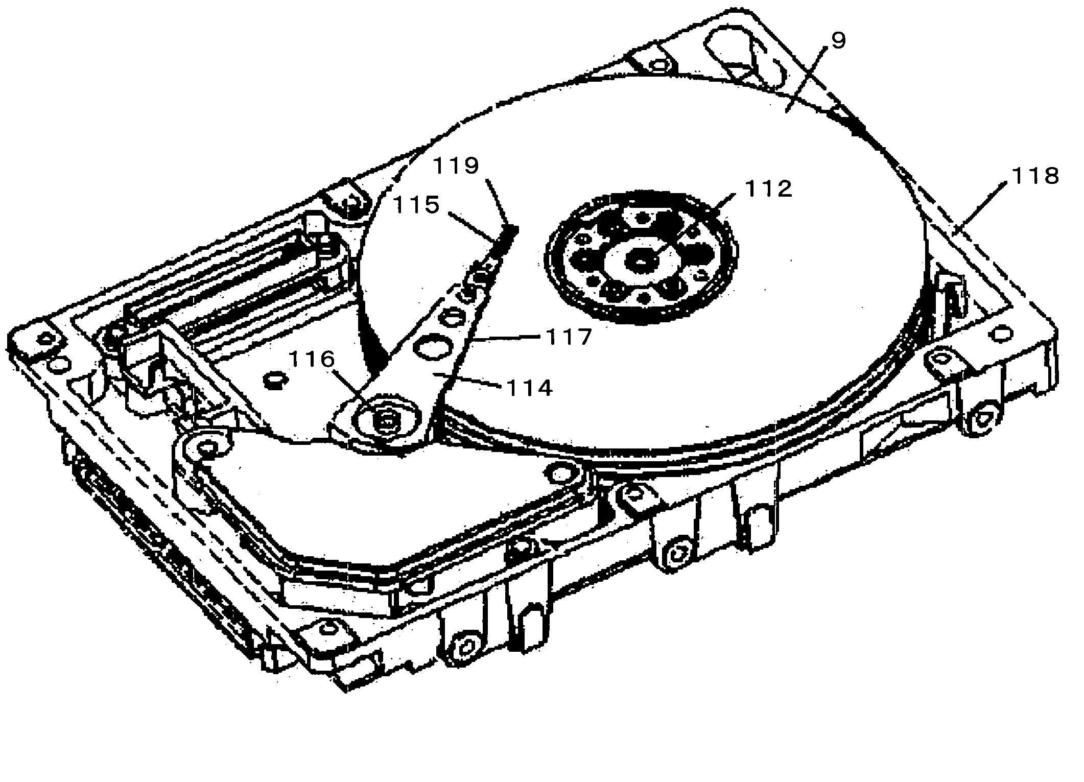
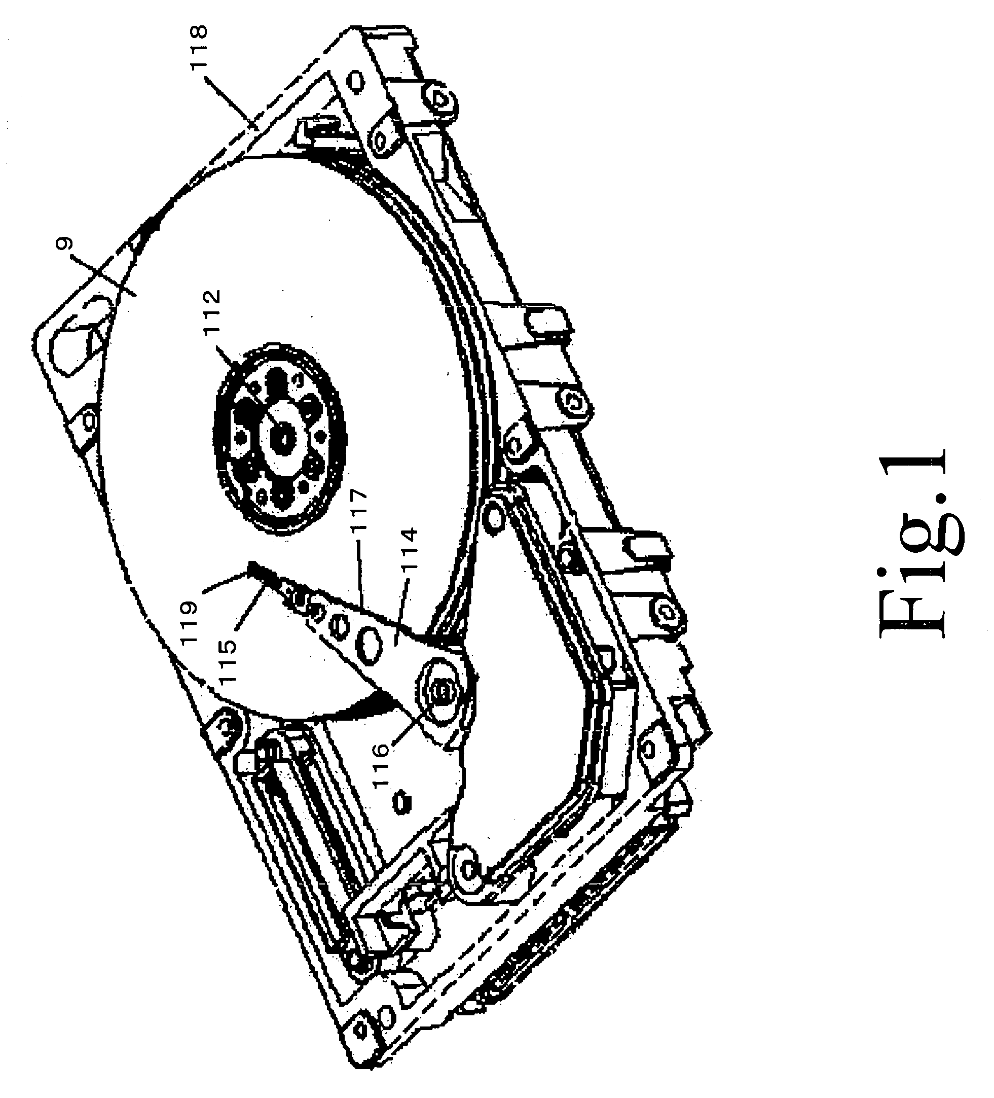
[0023]FIG. 1 is a perspective view of a magnetic disk apparatus. A magnetic disk 9 includes magnetic information and is rapidly rotated by a spindle motor 112. An actuator arm 114 is provided with a suspension 115 made of stainless steel. In addition, the actuator arm 114 is rotatably fixed to a housing 118 by a shaft 116 and is moved in a radius direction of the magnetic disk 9. Accordingly, a slider 119 fitted to the suspension 115 is moved over the magnetic disk 9, so that recording and reproducing of information are performed on a track. In the housing 118, a detection circuit device detecting a reproduced signal is fixed. The detection circuit device supplies a sense current to a magnetoresistive effect element in a read portion of a magnetic head and measures the change in voltage of the magnetoresistive effect element, so that information is reproduced from the magnetic disk 9.
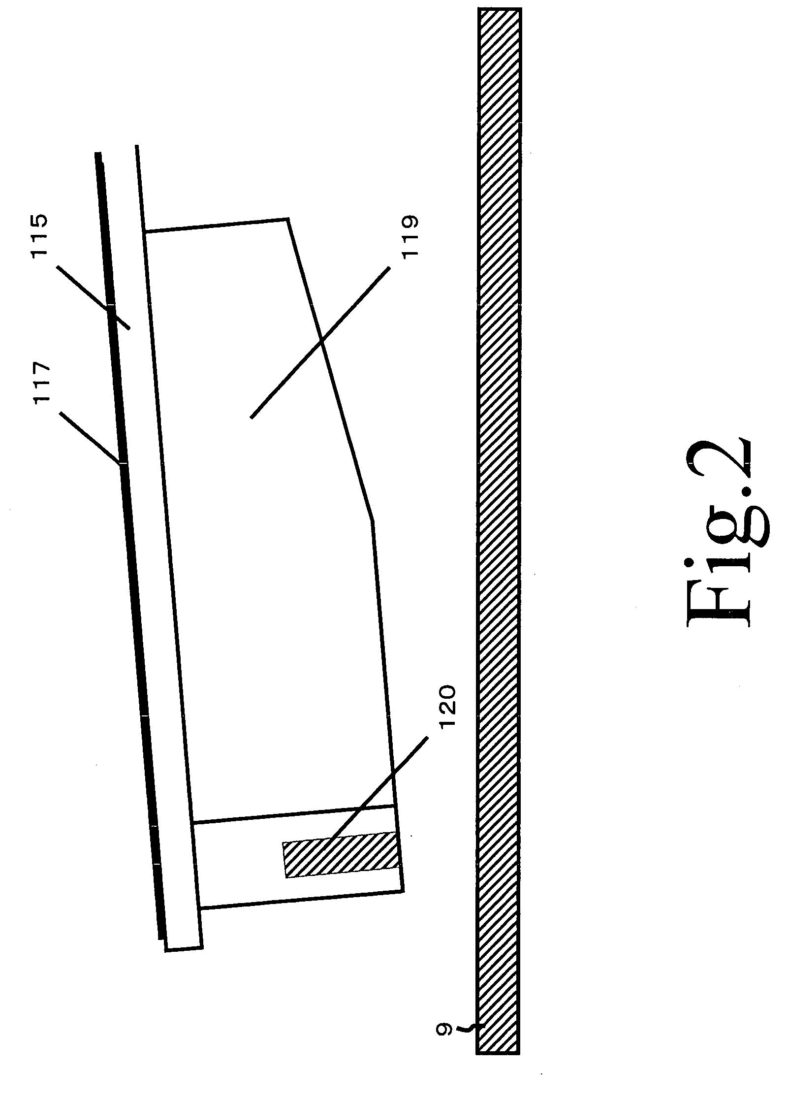
[0024]FIG. 2 is a schematic view showing the positional relationship among the magnetic disk 9, the ...
embodiment 2
[0034]In Embodiment 1, the structure is described in which the lower shield and electrode layer 6 and the upper shield and electrode layer 4 are formed to sandwich the magnetoresistive effect element 5 in the thickness direction; however, another structure may also be formed.
[0035]FIG. 7 is a cross-sectional view of a magnetic head 120 of Embodiment 2 taken along a direction perpendicular to an air bearing surface thereof. In this magnetic head 120, a lower shield and electrode layer 6 and an upper shield and electrode layer 4 are formed on a substrate 7 made of AlTiC (Al2O3—TiC) to sandwich a magnetoresistive effect element 5 in a lamination direction. In addition, an upper shield layer 14 is formed outside the upper shield and electrode layer 4. On the upper shield layer 14, a lower magnetic pole 2 of a write head is formed, and a writing coil 8 and an upper magnetic pole 1 are formed, so that the magnetic head 120 is formed.
[0036]The lower shield and electrode layer 6, the magnet...
PUM
| Property | Measurement | Unit |
|---|---|---|
| thickness | aaaaa | aaaaa |
| depth | aaaaa | aaaaa |
| width | aaaaa | aaaaa |
Abstract
Description
Claims
Application Information
 - R&D Engineer
- R&D Manager
- IP Professional
- Industry Leading Data Capabilities
- Powerful AI technology
- Patent DNA Extraction
Browse by: Latest US Patents, China's latest patents, Technical Efficacy Thesaurus, Application Domain, Technology Topic.
© 2024 PatSnap. All rights reserved.Legal|Privacy policy|Modern Slavery Act Transparency Statement|Sitemap