Semiconductor laser device

Active Publication Date: 2008-07-24
PANASONIC SEMICON SOLUTIONS CO LTD
View PDF9 Cites 7 Cited by
  • Summary
  • Abstract
  • Description
  • Claims
  • Application Information

AI Technical Summary

Benefits of technology

[0071]Thus, non-radiative recombination making no contribution to the laser oscillation can be reduced in the window region, and hence, heat generation of the device in the window region can be suppressed. As a result, a COD level can be prevented from lowering.
[0072]As described so far, according to the present invention, in a semiconductor laser device including a plurality of light emitting portions for light of, for example, a red region and an infrared region integrated on one substrate, the width of a ridge stripe is constant or gradually reduced toward a rear end face along the length of a resonator in a fro

Problems solved by technology

Also, in the case where a semiconductor laser is used in an optical disc apparatus, when the reflectance on the front end

Method used


Image

  • Semiconductor laser device
  • Semiconductor laser device
  • Semiconductor laser device

Examples


Example

[0085]A semiconductor laser device according to an embodiment of the invention will now be described with reference to the accompanying drawings.

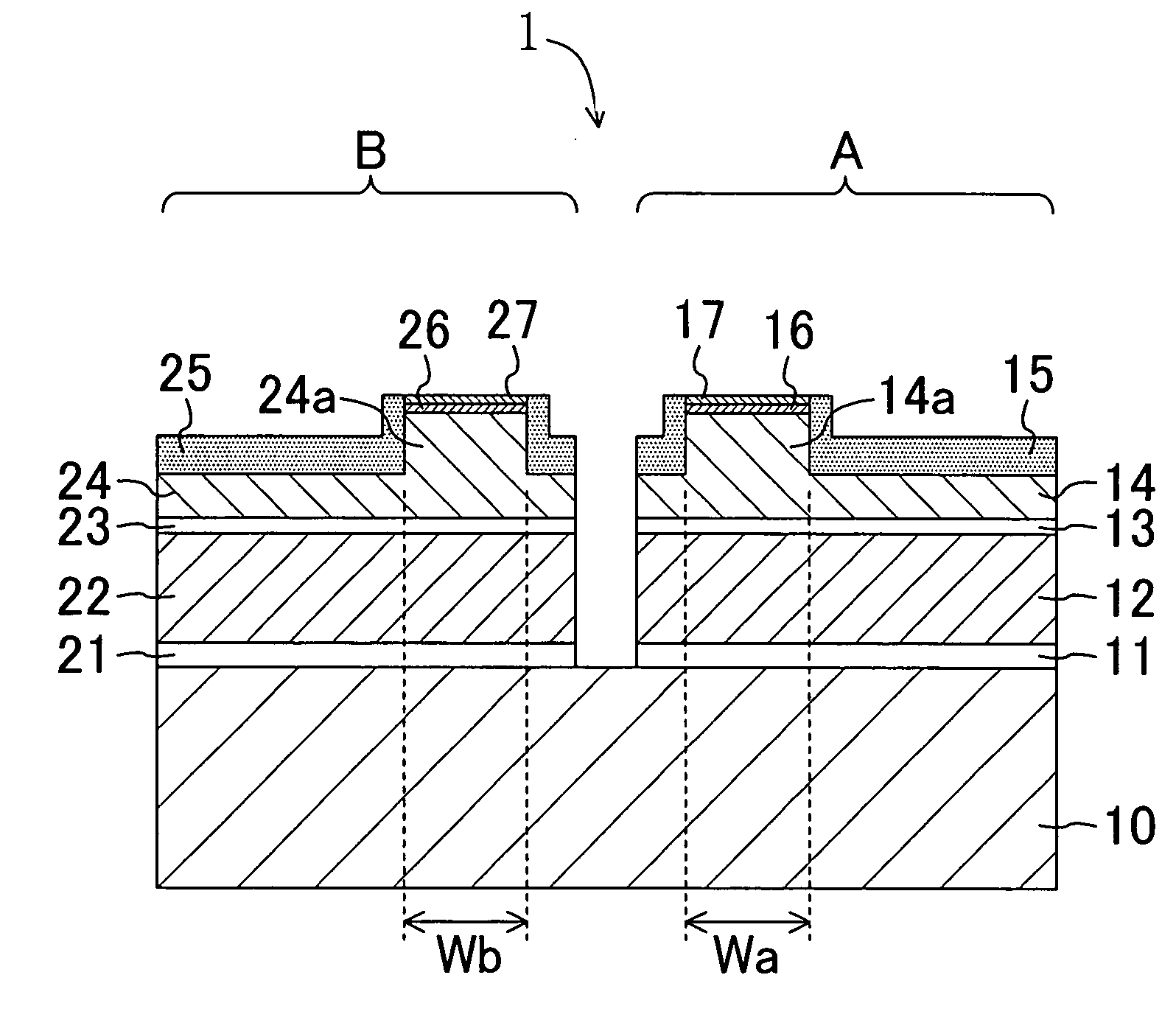
[0086]FIG. 1A is a schematic cross-sectional view of a semiconductor laser device 1 of this embodiment.

[0087]In the semiconductor laser device 1, a red laser A and an infrared laser B are integrated, as two light emitting portions for emitting light of different wavelengths, on an n-type GaAs substrate 10 having, as the principal plane, a plane inclined from the (100) plane by 10 degrees along the [011] direction. First, the structure of the red laser A will be described.

[0088]The red laser A has a structure in which an n-type buffer layer 11 (with a thickness of 0.5 μm) made of n-type GaAs, an n-type cladding layer 12 (with a thickness of 2.0μ) made of n-type (Al0.7Ga0.3)0.51In0.49P, an active layer 13 having a strained quantum well structure, a p-type cladding layer 14 made of p-type (Al0.7Ga0.3)0.51In0.49P, a p-type intermediate layer 16...


PUM


Abstract

The semiconductor laser device includes first and second light emitting portions each including a first cladding layer, an active layer and a second cladding layer, and each having a stripe structure. The stripe structure of the first light emitting portion has a section having a width changing along a resonator direction and includes a first front end face, and relationships of Wf1≧W1; W1>W2; and (Wf1−W1)/2L1<(W1−W2)/2L2 hold wherein Wf1 is a width on the first front end face; W1 is a width in a position away from the first front end face by a distance L1; and W2 is a width in a position away from said the front end face by a distance L1+L2 (whereas L1+L2≦L). The stripe structure of the second first light emitting portion has a section having a width changing along a resonator direction and includes a second front end face, and relationships of Wf2≧W3; W3>W4; and (Wf2−W3)/2L3<(W3−W4)/2L4 hold wherein Wf2 is a width on the second front end face; W1 is a width in a position away from the second front end face by a distance L3 (whereas L1≠L3); and W4 is a width in a position away from the second front end face by a distance L3+L4.

Description

CROSS-REFERENCE TO RELATED APPLICATIONS[0001]This application claims priority under 35 U.S.C. § 119 on Patent Application No. 2006-242513 filed in Japan on Sep. 7, 2006, the entire contents of which are hereby incorporated by reference.BACKGROUND OF THE INVENTION[0002]The present invention relates to a semiconductor laser device, and more particularly, it relates to a semiconductor laser device applicable to two wavelengths of a red region and an infrared region.[0003]Currently, digital video discs (DVDs) capable of high density recording and having large capacity and DVD apparatuses for recording / reproducing data in / from DVDs are commercially available, and they are regarded as products expected to be in larger demand from now on. Since data is recorded in a high density in a DVD, an AlGaInP-based semiconductor laser of an emission wavelength of 650 nm is used as a laser light source for the recording / reproducing. Therefore, in an optical pickup of a conventional DVD apparatus, a C...

Claims


Application Information

Patent Timeline
IPC IPC(8): H01S5/22
CPCH01S5/028H01S5/0287H01S5/1039H01S5/4087H01S5/162H01S5/22H01S5/4031H01S5/1064H01S5/00H01S5/14
Inventor TAKAYAMA, TORUSATOH, TOMOYAHAYAKAWA, KOICHIKIDOGUCHI, ISAO
Owner PANASONIC SEMICON SOLUTIONS CO LTD
Why Eureka
Try Eureka