Organic light emitting diode pixel array
a light-emitting diode and organic technology, applied in the field of organic light-emitting diodes (oled) pixel arrays, can solve the problems of excessive spatial frequency of transmittance regions and unfavorable imaging quality, and achieve the effect of satisfying image definition
- Summary
- Abstract
- Description
- Claims
- Application Information
AI Technical Summary
Benefits of technology
Problems solved by technology
Method used
Image

Examples
first embodiment
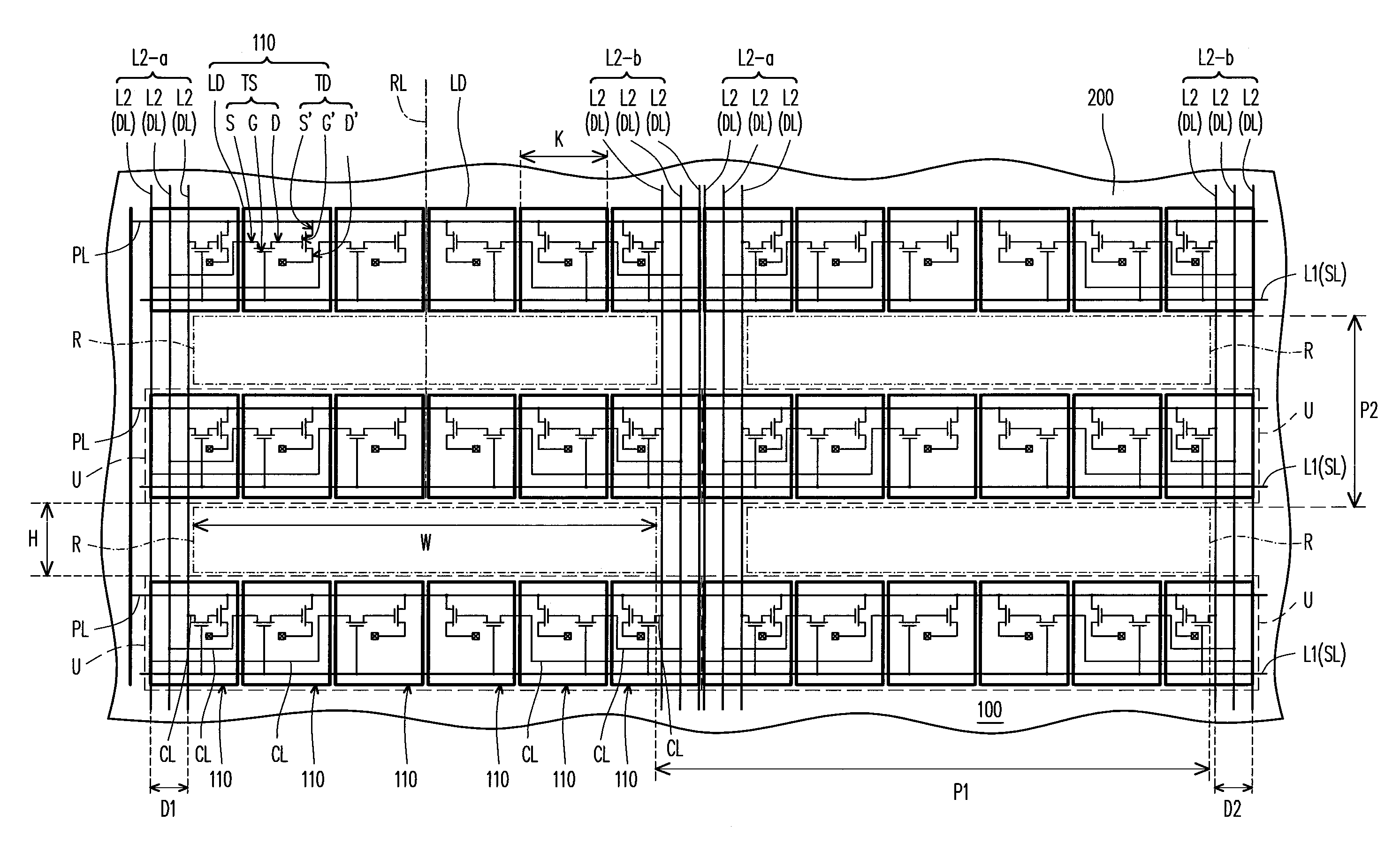
[0017]FIG. 1 is a schematic view illustrating an OLED pixel array 100 according to a first embodiment of the invention. With reference to FIG. 1, the OLED pixel array 100 of this embodiment is configured on a substrate 200 and includes a plurality of first signal lines L1, a plurality of second signal lines L2, and a plurality of pixel array units U. The substrate 200 of this embodiment carries devices thereon, and the substrate 200 can be made of glass, quartz, organic polymer, or any other appropriate material.
[0018]The first signal lines L1 intersect the second signal lines L2. Here, when the first signal lines L1 are scan lines SL, the second signal lines L2 are data lines DL, and when the first signal lines L1 are the data lines DL, the second signal lines L2 are the scan lines SL. According to this embodiment, the first signal lines L1 are the scan lines SL, and the second signal lines L2 are the data lines DL. Here, the first signal lines L1 (i.e., the scan lines SL) intersec...
second embodiment
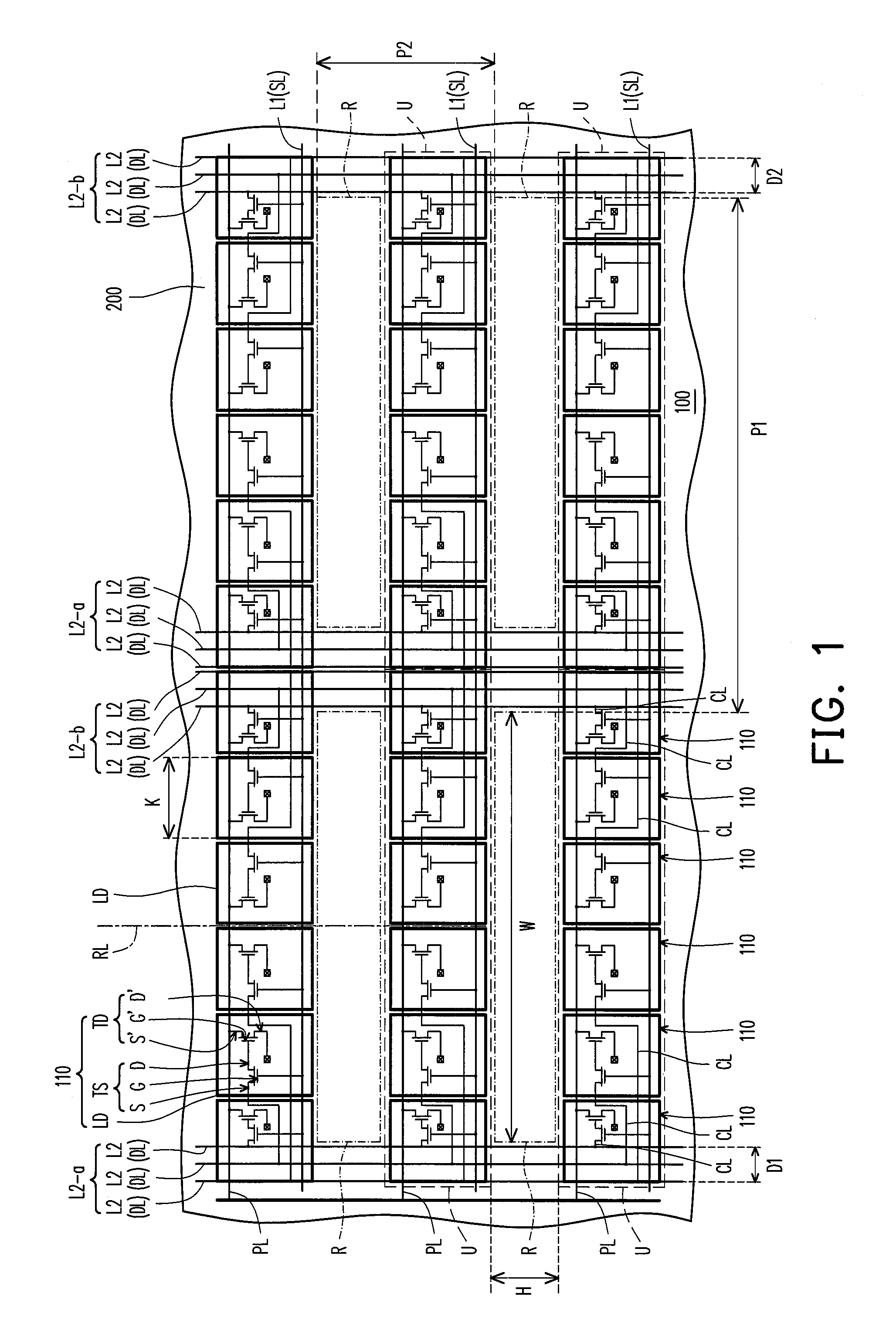
[0030]FIG. 2 is a schematic view illustrating an OLED pixel array 100A according to a second embodiment of the invention. With reference to FIG. 2, the OLED pixel array 100A of this embodiment is similar to the OLED pixel array 100 of the first embodiment as shown in FIG. 1, and therefore the same elements in FIG. 2 and FIG. 1 are represented by the same reference numerals or symbols. The difference therebetween is described below, while the similarity therebetween is omitted herein.
[0031]In the OLED pixel array 100A of this embodiment, the OLED pixels 110 are located between the first portion L2-a and the second portion L2-b of the second signal lines L2. Here, a transmittance region R is surrounded by the first portion L2-a, the second portion L2-b, and the OLED pixels 110, and the first portion L2-a and the second portion L2-b are respectively located at two opposite sides of the transmittance region R. Specifically, the difference between the OLED pixel array 100A of this embodi...
third embodiment
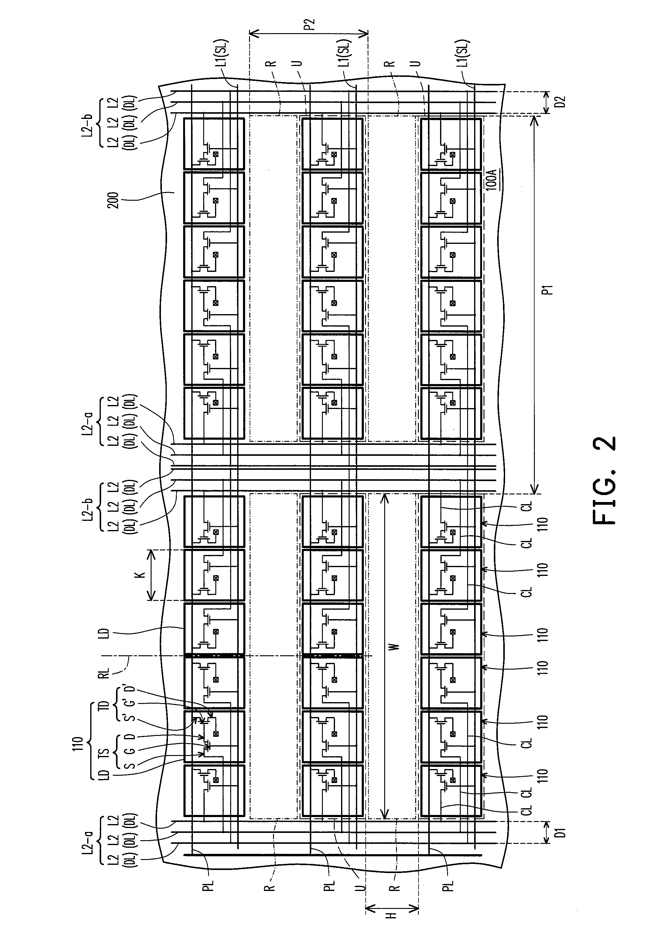
[0033]FIG. 3 is a schematic view illustrating an OLED pixel array 100B according to a third embodiment of the invention. With reference to FIG. 3, the OLED pixel array 100B of this embodiment is similar to the OLED pixel array 100 of the first embodiment as shown in FIG. 1, and therefore the same elements in FIG. 3 and FIG. 1 are represented by the same reference numerals or symbols. The difference therebetween is described below, while the similarity therebetween is omitted herein.
[0034]The difference between the OLED pixel array 100B of this embodiment and the OLED pixel array 100 of the first embodiment lies in that the first signal lines L1 are the data lines DL, and the second signal lines L2 are the scan lines SL. Since the OLED pixel array 100B of this embodiment is similar to the OLED pixel array 100 of the first embodiment except for the above-mentioned difference, no further description is given herein. That is to say, in each of the OLED pixels 110, the gate G of the swit...
PUM
 Abstract
Description
Claims
Application Information
 - R&D Engineer
- R&D Manager
- IP Professional
- Industry Leading Data Capabilities
- Powerful AI technology
- Patent DNA Extraction
Browse by: Latest US Patents, China's latest patents, Technical Efficacy Thesaurus, Application Domain, Technology Topic.
© 2024 PatSnap. All rights reserved.Legal|Privacy policy|Modern Slavery Act Transparency Statement|Sitemap