
Semiconductor memory devices having variable additive latency

a memory device and additive latency technology, applied in the field of semiconductor memory devices, can solve the problems of data dq not being output continuously, data line bandwidth loss, data output bubbles, etc., and achieve the effect of improving data and command line efficiency

Active Publication Date: 2008-01-31
SAMSUNG ELECTRONICS CO LTD
View PDF6 Cites 9 Cited by
  • Summary
  • Abstract
  • Description
  • Claims
  • Application Information

AI Technical Summary

Benefits of technology

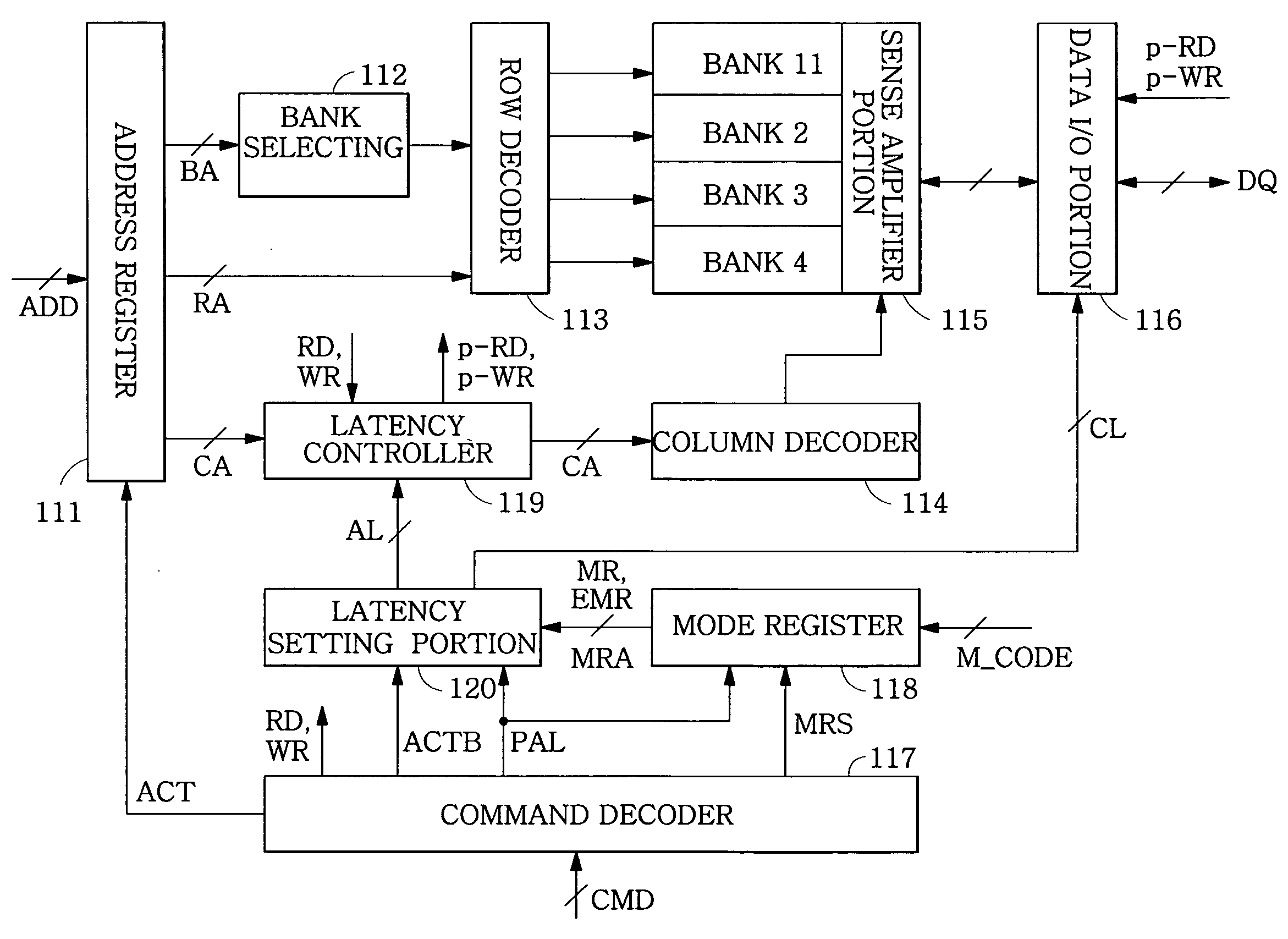
[0033]At least one example embodiment provides a semiconductor memory device in which the additive latency may be changed during normal operation so that efficiency of the data and command lines may be improved.

Problems solved by technology

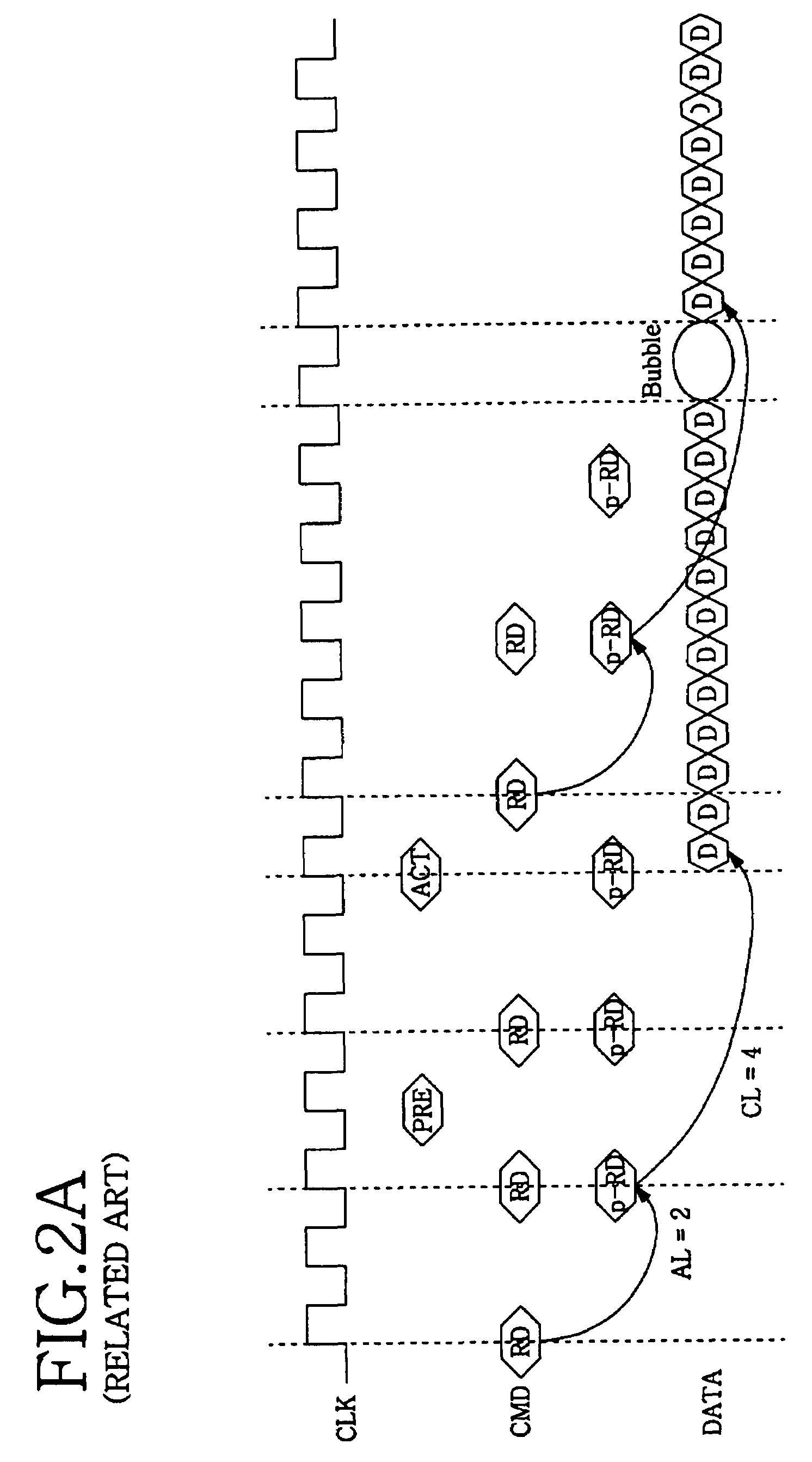
However, as shown in FIG. 2A, when the read command RD is not applied continuously, data DQ are not output continuously and bubbles may occur.
Bubbles may result in a loss of data line bandwidth through which data is output.
However, bubbles of the read command RD may result in loss of command line bandwidth.
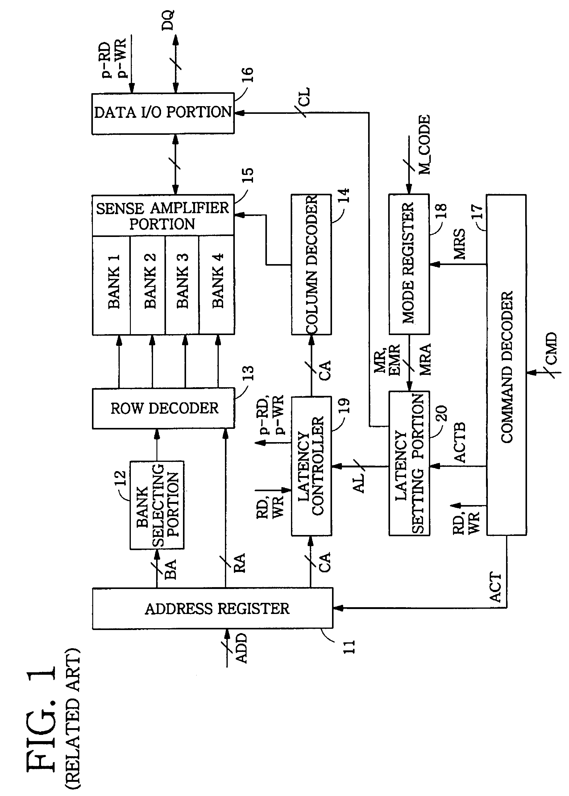
However, because the additive latency AL of the existing semiconductor memory device may be changed only when all banks are in the pre-charge state, it is inefficient because the change requires a longer time to adjust the additive latency AL.

Method used


Image

  • Semiconductor memory devices having variable additive latency
  • Semiconductor memory devices having variable additive latency
  • Semiconductor memory devices having variable additive latency

Examples


Embodiment Construction

[0045]Various example embodiments of the present invention will now be described more fully with reference to the accompanying drawings in which some example embodiments of the invention are shown. In the drawings, the thicknesses of layers and regions are exaggerated for clarity.

[0046]Detailed illustrative embodiments of the present invention are disclosed herein. However, specific structural and functional details disclosed herein are merely representative for purposes of describing example embodiments of the present invention. This invention may, however, may be embodied in many alternate forms and should not be construed as limited to only the embodiments set forth herein.

[0047]Accordingly, while example embodiments of the invention are capable of various modifications and alternative forms, embodiments thereof are shown by way of example in the drawings and will herein be described in detail. It should be understood, however, that there is no intent to limit example embodiments...


PUM


Abstract

A semiconductor memory device includes an additive latency setting unit configured to receive a mode setting code from an external unit in response to the mode setting signal during a mode setting operation, set an additive latency value in response to the mode setting code, and receive the mode setting code in response to the additive latency setting signal during a normal operation, and an additive latency changing unit configured to change the additive latency value in response to the mode setting code during the normal operation.

Description

PRIORITY STATEMENT[0001]This non-provisional U.S. patent application claims priority under 35 U.S.C. §119 to Korean Patent Application No. 2006-0064100, filed Jul. 7, 2006, the entire contents disclosure of which are incorporated herein by reference.BACKGROUNDDescription of the Related Art [0002]Related art semiconductor memory devices may have CAS latency CL and / or additive latency AL. CAS latency represents the number of clocks until data are output to an external portion after a read command is input to a memory device. For example, a CAS latency of 3 indicates data are output to the external portion 3 clock cycles lapse after a read command is input to the memory device. The CAS latency value represents timing for outputting data. The memory device detects the CAS latency value set during an initial operation, and uses the detected CAS latency value to access and output data.[0003]Additive latency is discussed in DDR2 specifications and represents the number of clocks from input...

Claims


Application Information

Patent Timeline
Patent Type & Authority Applications(United States)
IPC IPC(8): G11C7/00G11C8/00
CPCG11C7/1045G11C2207/2272G11C7/22G11C7/20
Inventor YU, SO-YOUNGLEE, JAE-KYUNG
Owner SAMSUNG ELECTRONICS CO LTD
Learn More