Semiconductor memory device

a memory device and semiconductor technology, applied in the direction of semiconductor devices, semiconductor/solid-state device details, radiation control devices, etc., can solve the problems of 64-bit computer chips needing more devices, laterally oriented devices consuming significant amounts of chip area, and increasing the cost of manufacturing equipmen

Inactive Publication Date: 2008-02-07
BESANG
View PDF33 Cites 249 Cited by
  • Summary
  • Abstract
  • Description
  • Claims
  • Application Information

AI Technical Summary

Problems solved by technology

However, these laterally oriented devices consume significant amounts of chip area.
However, the 64-bit computer chip will need more devices since there are more bits to process at a given time.
The number of devices can be increased by making the devices included therein smaller, but this requires advances in lithography and increasingly expensive manufacturing equipment.
However, the yield of the computer chips fabricated in a run decreases as their area increases, which increases the overall cost.
However, there are several problems with doing this.
One problem is that the masks used to fabricate the memory devices are not compatible with the masks used to fabricate the other devices on the computer chip.
Hence, it is more complex and expensive to fabricate a computer chip with memory embedded in this way.
Another problem is that memory devices tend to be large and occupy a significant amount of area.
The total area of the computer chip can be increased, but as discussed above, this decreases the yield and increases the cost.

Method used


Image

  • Semiconductor memory device
  • Semiconductor memory device
  • Semiconductor memory device

Examples


Embodiment Construction

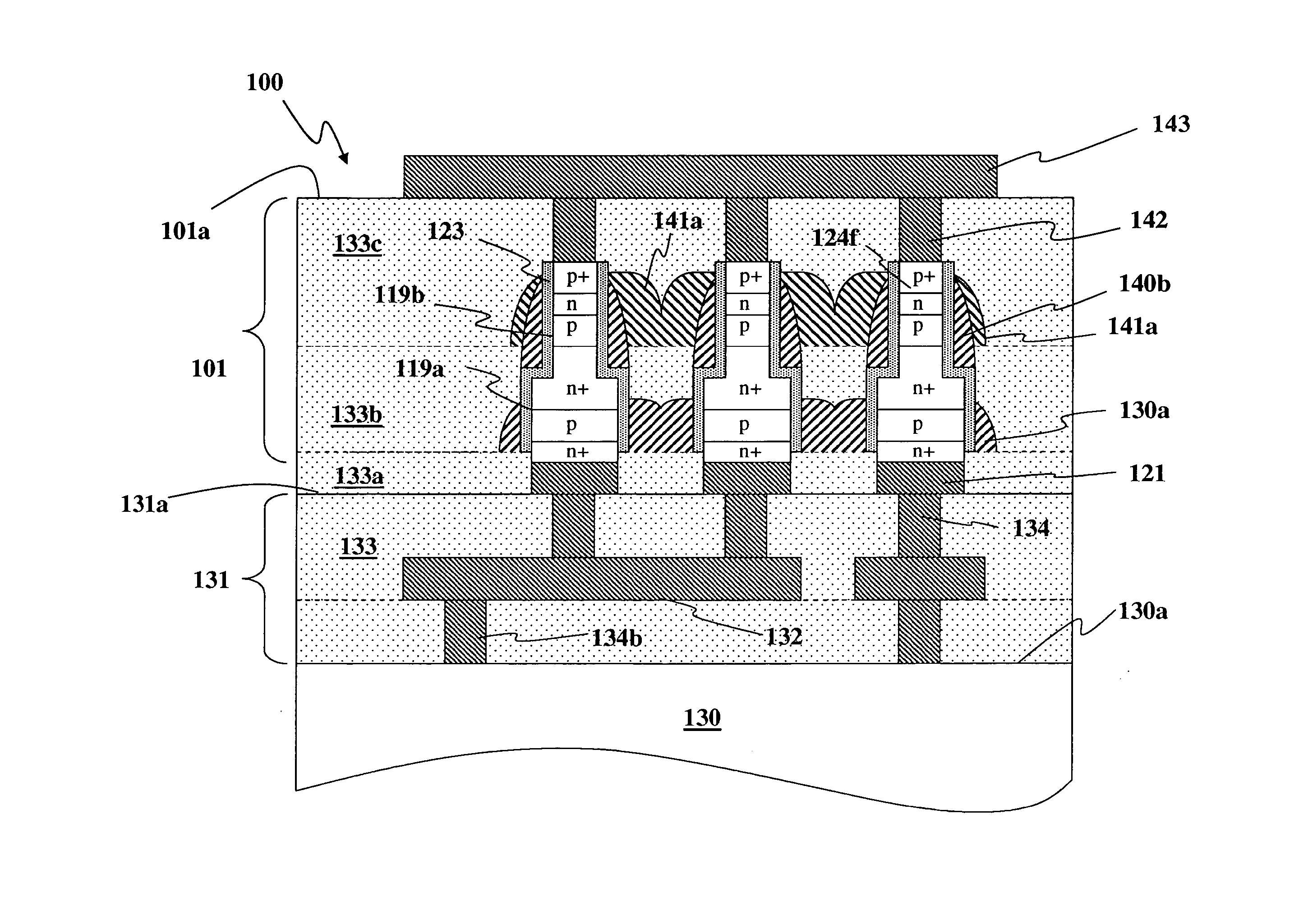
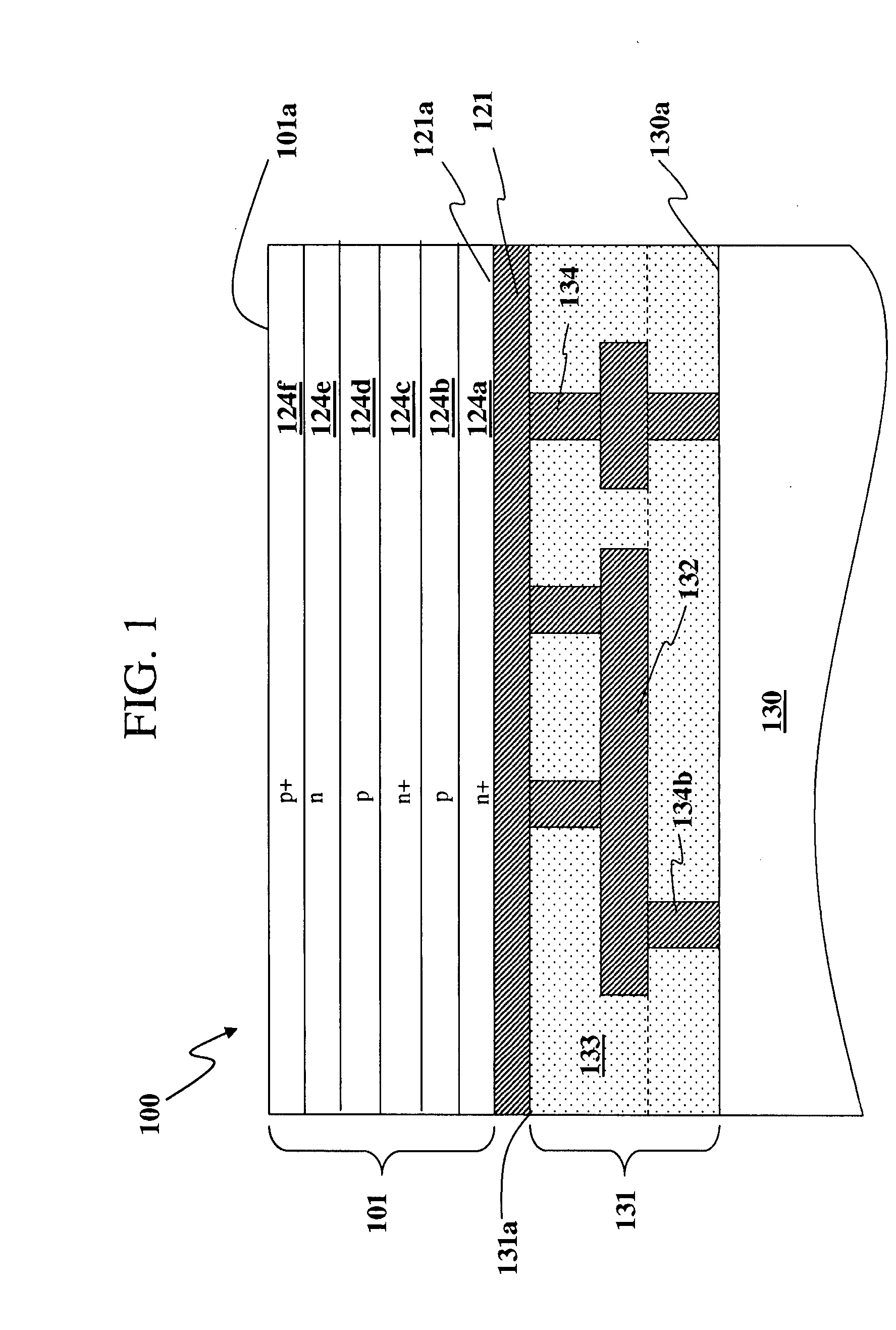
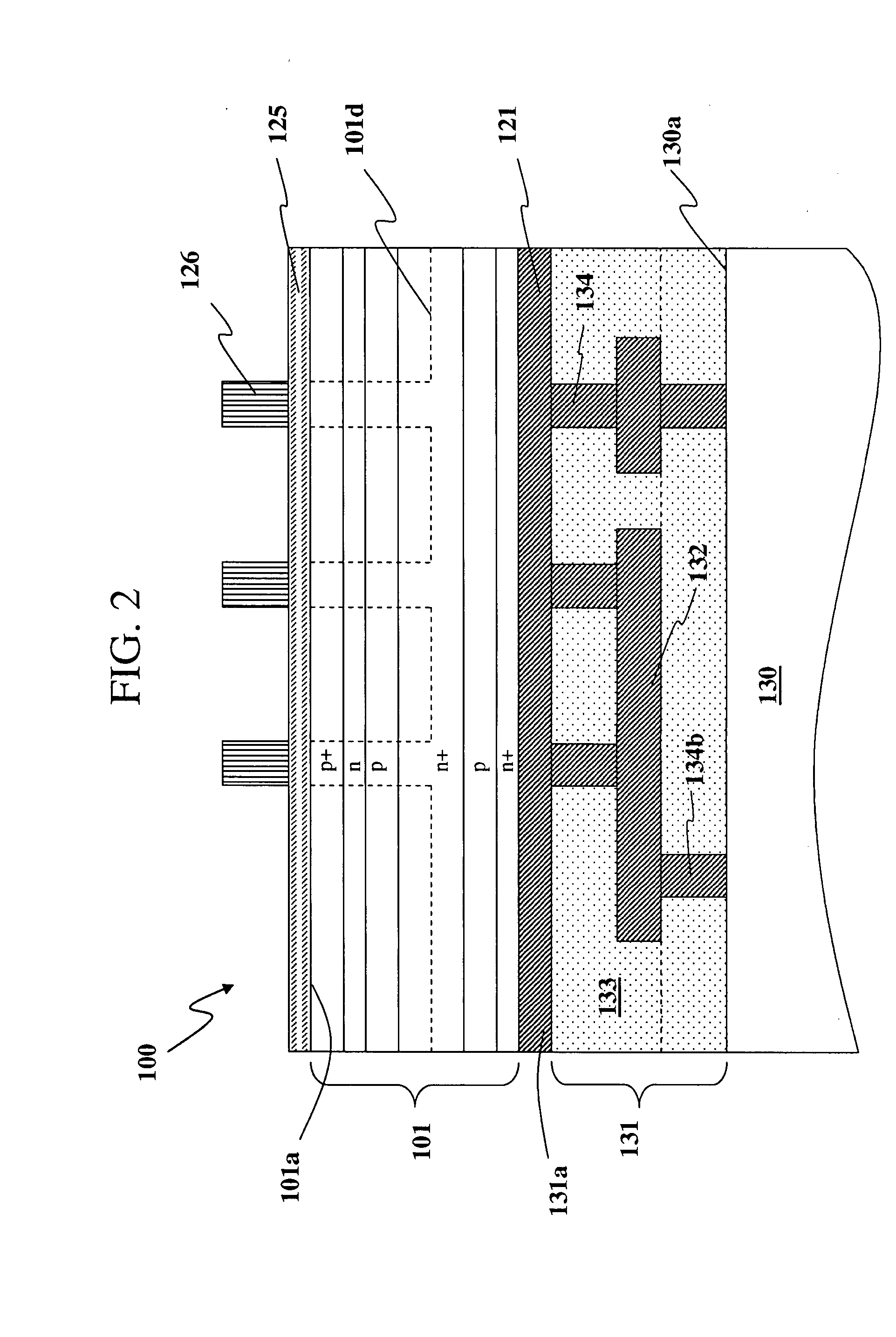
[0017]FIGS. 1-12 are simplified sectional views of steps in fabricating a semiconductor memory circuit 100 in accordance with the present invention. In the following figures, like reference characters indicate corresponding elements throughout the several views. In FIGS. 1-12, only a few memory devices are shown in circuit 100, but it should be understood that circuit 100 generally includes a number of memory devices and that only a few are shown for simplicity and ease of discussion.

[0018] Circuit 100 can be included in a computer chip where the memory devices are positioned above the computer circuitry. The memory devices are typically coupled to the computer circuitry through interconnects which include a conductive line and / or a conductive via. Circuit 100 has several advantages. One advantage is that the memory devices are positioned above the computer circuitry which is desirable since the memory devices typically occupy much more area than the computer circuitry. Another adv...


PUM


Abstract

A method of forming a circuit includes providing a substrate; providing an interconnect region positioned on the substrate; bonding a device structure to a surface of the interconnect region; and processing the device structure to form a first stack of layers on the interconnect region and a second stack of layers on the first stack. The width of the first stack is different than the width of the second stack.

Description

CROSS REFERENCE TO RELATED APPLICATIONS [0001] This is a divisional of application Ser. No. 11 / 092,500, entitled “SEMICONDUCTOR MEMORY DEVICE”, filed on Mar. 29, 2005, which claims priority to U.S. Pat. No. 7,052,941 filed on Jun. 21, 2004, the contents of both of which are incorporated herein by reference.BACKGROUND OF THE INVENTION [0002] 1. Field of the Invention [0003] This invention relates generally to semiconductor circuitry and, more particularly, to semiconductor memory devices. [0004] 2. Description of the Related Art[0005] Advances in semiconductor manufacturing technology have provided computer chips with integrated circuits that include many millions of active and passive electronic devices, along with the interconnects to provide the desired circuit connections. As is well-known, most integrated circuits include laterally oriented active and passive electronic devices that are carried on a single major surface of a substrate. Active devices typically include transistor...

Claims


Application Information

Patent Timeline
Patent Type & Authority Applications(United States)
IPC IPC(8): H01L21/332H01L21/20H01L21/30H01L21/336H01L21/46H01L21/58H01L23/48H01L27/108H01L27/148
CPCH01L21/2007H01L21/8221H01L2924/1301H01L2924/1306H01L2924/01033H01L24/83H01L27/0688H01L27/1027H01L27/11H01L27/11551H01L29/742H01L2224/291H01L2224/8385H01L2924/01005H01L2924/01013H01L2924/01015H01L2924/01018H01L2924/01027H01L2924/01029H01L2924/01038H01L2924/01056H01L2924/01073H01L2924/01074H01L2924/01075H01L2924/01078H01L2924/01079H01L2924/07802H01L2924/13091H01L2924/14H01L2924/1433H01L2924/19041H01L2924/19042H01L2924/19043H01L2924/30105H01L2924/3011H01L24/29H01L2924/01006H01L2924/01019H01L2924/00H01L2924/12036H01L23/48H10B10/00H10B41/20
Inventor LEE, SANG-YUN
Owner BESANG
Why Eureka
Try Eureka