Supercharge Your Innovation With Domain-Expert AI Agents!

Method of Manufacturing Image Sensor

a manufacturing method and sensor technology, applied in the direction of semiconductor devices, semiconductor/solid-state device details, electrical devices, etc., can solve the problems of insufficient amount of light reaching the photoelectric converter, low sensitivity, and light incident on the photoelectric converter to be markedly reduced

Inactive Publication Date: 2008-02-14
SAMSUNG ELECTRONICS CO LTD
View PDF4 Cites 56 Cited by
  • Summary
  • Abstract
  • Description
  • Claims
  • Application Information

AI Technical Summary

Problems solved by technology

However, with a conventional CMOS image sensor, an insufficient amount of light may reach the photoelectric converter due to the layout of the multi-layer wiring line.
For example, the layout of the multi-layer wiring line may reduce the aperture ratio of the photoelectric converter, which thereby may cause light incident on the photoelectric converter to be markedly reduced, resulting in low sensitivity.

Method used


Image

  • Method of Manufacturing Image Sensor
  • Method of Manufacturing Image Sensor
  • Method of Manufacturing Image Sensor

Examples


Embodiment Construction

[0019] The present invention may, however, be embodied in many different forms and should not be construed as being limited to the exemplary embodiments set forth herein. Rather, these embodiments are provided so that this disclosure will be thorough and complete and will fully convey the concept of the invention to those skilled in the art, and the present invention will only be defined by the appended claims. Like reference numerals refer to like elements throughout the specification.

[0020] An exemplary embodiment of the present invention will now be described more fully with reference to the accompanying drawings.

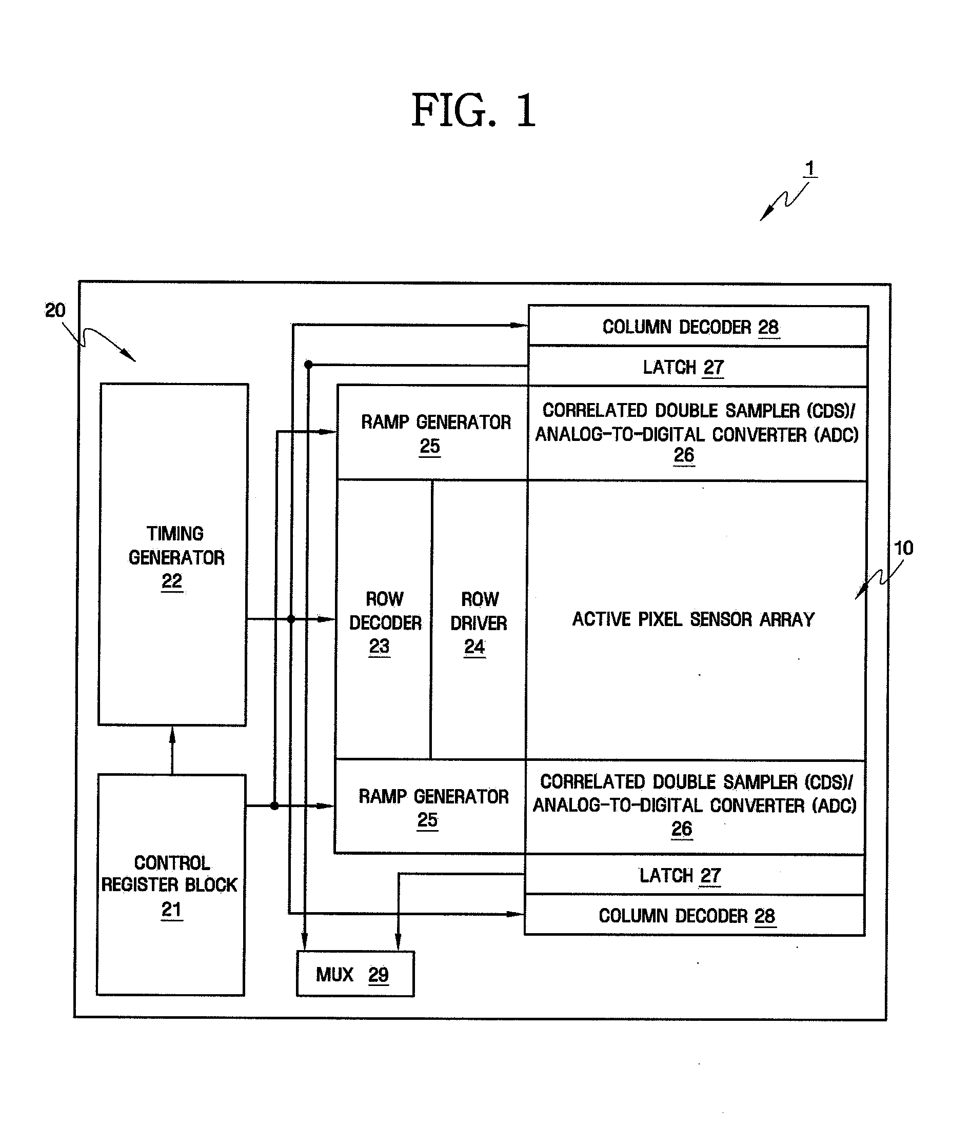
[0021]FIG. 1 is a block diagram illustrating an image sensor according to an exemplary embodiment of the present invention.

[0022] Referring to FIG. 1, an image sensor 1 according to an exemplary embodiment of the invention includes two main areas, that is, an active pixel sensor area 10 and a peripheral circuit area 20.

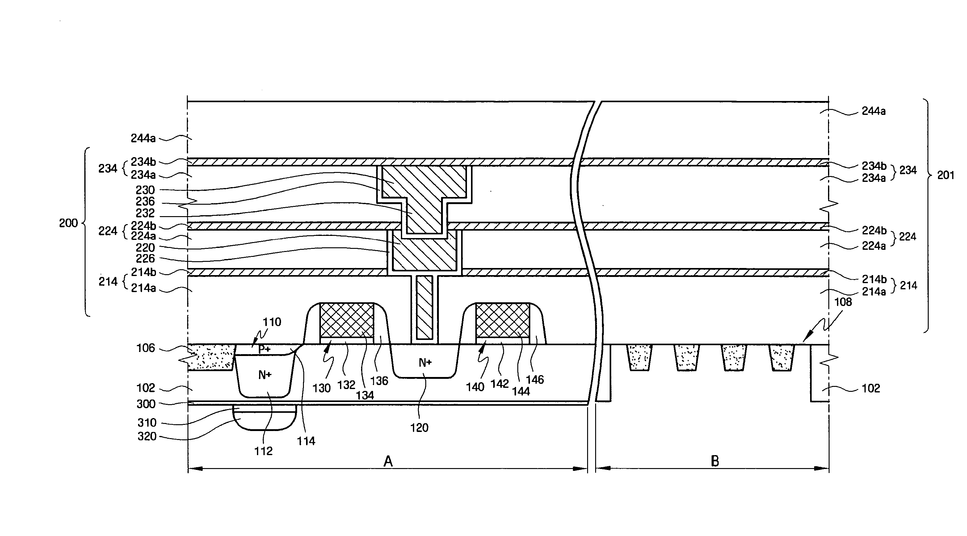
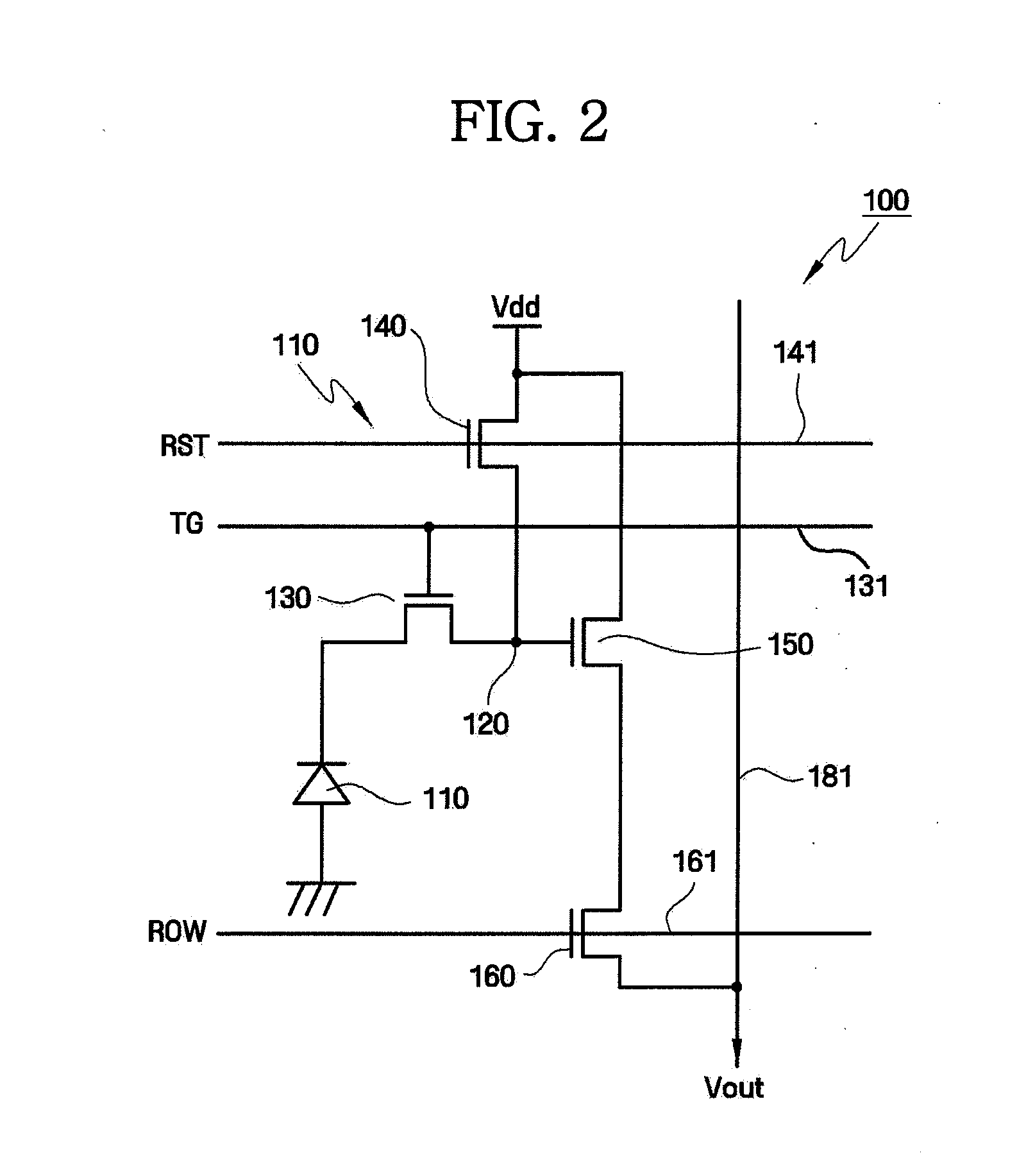
[0023] The active pixel sensor area 10 includes ...


PUM


Abstract

A method of manufacturing an image sensor includes forming a device isolation region in an active pixel sensor area of a semiconductor substrate and alignment keys in a scribe lane area of the semiconductor substrate, such that the depth of the alignment keys is equal to or shallower than the depth of the device isolation region. The method further includes forming a photoelectric converter in the active pixel sensor area, polishing a rear surface of the semiconductor substrate and using the alignment keys to form a microlens at a position corresponding to the photoelectric converter on the polished rear surface of the semiconductor substrate.

Description

[0001] This application claims priority from Korean Patent Application No. 10-2006-0075825 filed on Aug. 10, 2006, the disclosure of which is hereby incorporated by reference herein in its entirety. BACKGROUND OF THE INVENTION [0002] 1. Technical Field [0003] The present disclosure relates to a method of manufacturing an image sensor, and more particularly, to a method of manufacturing an image sensor capable of using alignment keys formed in a scribe lane area. [0004] 2. Description of the Related Art [0005] Image sensors are semiconductor devices for converting incident light into electric signals. The image sensors may be divided into two main types of, for example,charge coupled devices (CCDs) and complementary metal oxide semiconductors (CMOS) image sensors. [0006] A charge coupled device may have metal oxide semiconductors (MOS) capacitors adjacent to one another, and the MOS capacitor stores charge and transfers the charge. Meanwhile, the CMOS image sensor may have a pluralit...

Claims


Application Information

Patent Timeline
IPC IPC(8): H01L31/18
CPCH01L27/14609H01L27/14621H01L27/14627H01L27/1464H01L27/14687H01L27/14689H01L27/14636H01L27/14
Inventor YOO, GIL-SANGPARK, BYUNG-JUNLEE, YUN-KI
Owner SAMSUNG ELECTRONICS CO LTD
Features
  • R&D
  • Intellectual Property
  • Life Sciences
  • Materials
  • Tech Scout
  • Unparalleled Data Quality
  • Higher Quality Content
  • 60% Fewer Hallucinations
Learn More