Method and system for continuous large-area scanning implantation process

a large-area scanning and implantation process technology, applied in the direction of sustainable manufacturing/processing, final product manufacturing, transportation and packaging, etc., can solve the problems of difficult manufacturing, low efficiency of solar cells, and many limitations of solar cells, so as to reduce the channeling effect of implanted ions

Inactive Publication Date: 2008-02-14
SILICON GENERAL CORPORATION
View PDF99 Cites 115 Cited by
  • Summary
  • Abstract
  • Description
  • Claims
  • Application Information

AI Technical Summary

Benefits of technology

[0015] As merely an example, the tray member may be provided in a vertical position, or an upside-down position, or in an angled orientation in relation to a direction of implantation (e.g., direction of ions being implanted into the reusable substrates) in certain embodiments for controlling channeling effects of the implanted species into the reusable substrates. In silicon implantation for example, implant angle of approximately 7 degrees off of (100) surface normal is routinely utilized to reduce channeling effects of the implanted ions present during an implant along a major crystallographic direction. Alternatively, the reusable substrate can be cut at an angle off of the major crystallographic direction to accomplish the same result when implanted in a perpendicular implant geometry. In a specific embodiment, the tray can face a direction away from direct gravitational force, although there may be variations. In a preferred embodiment, the plurality of reusable substrates can be subjected to an scanning implant process. The plurality of reusable substrates may further be subjected to a bond and / or a controlled cleave process, together or separately. In a specific embodiment, the plurality of substrates may be processed to form p-n junctions in each of the plurality of substrates.

Problems solved by technology

Unfortunately, such petroleum sources have become depleted and have lead to other problems.
Although effective, these solar cells still have many limitations.
These materials are often difficult to manufacture as implantation processes may be inefficient and not optimal for such application.
Although these plates may be formed effectively, they do not possess optimum properties for highly effective solar cells.
Such single crystal silicon is, however, expensive and is also difficult to use for solar applications in an efficient and cost effective manner.
Generally, thin-film solar cells are less expensive by using less silicon material but their amorphous or polycrystalline structure are less efficient than the more expensive bulk silicon cells made from single-crystal silicon substrates.

Method used


Image

  • Method and system for continuous large-area scanning implantation process
  • Method and system for continuous large-area scanning implantation process
  • Method and system for continuous large-area scanning implantation process

Examples


Embodiment Construction

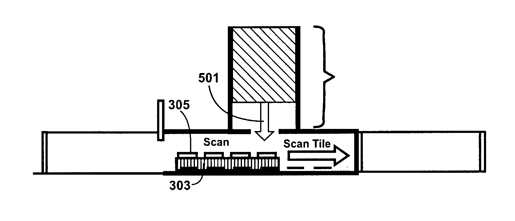
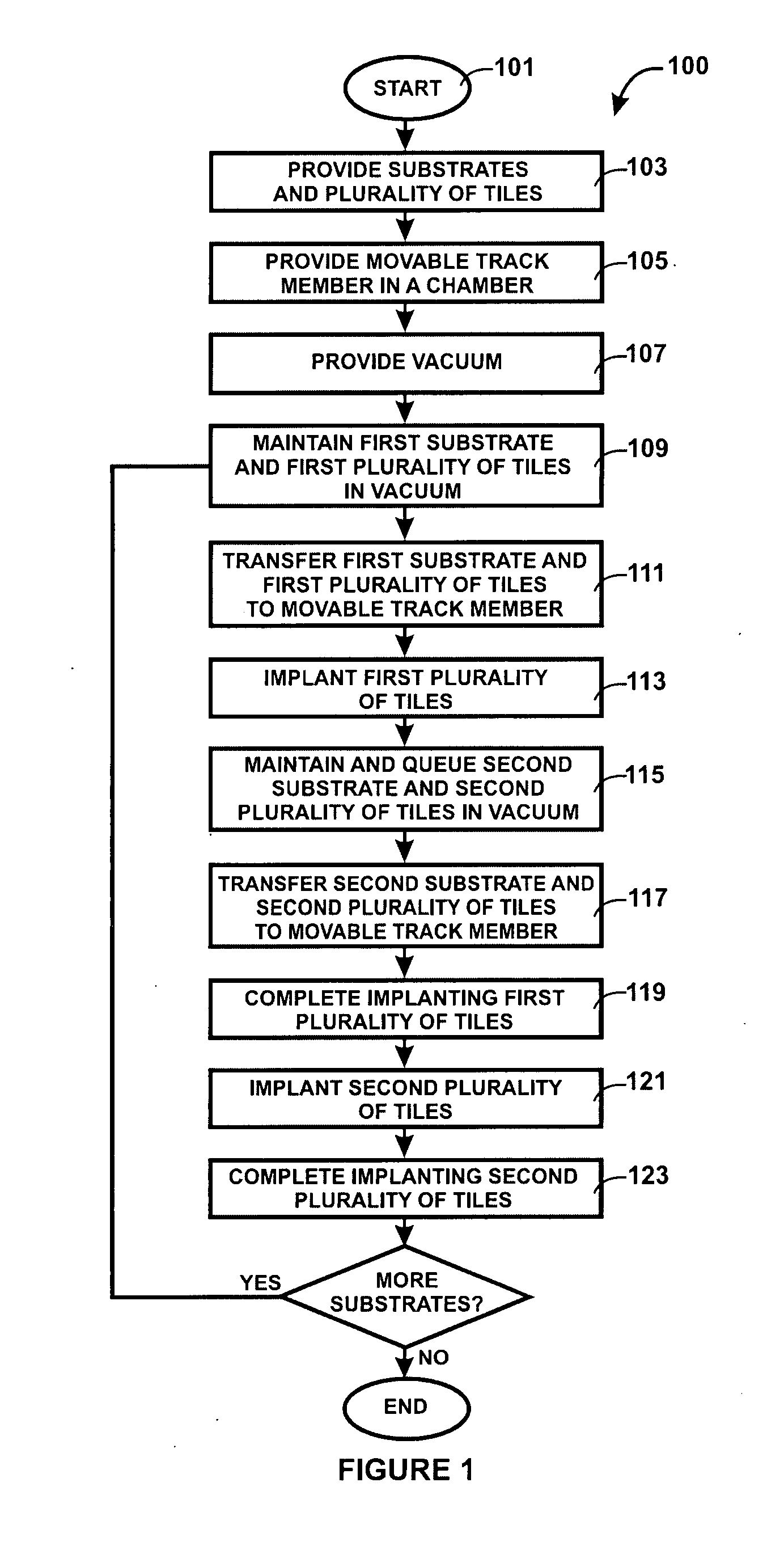
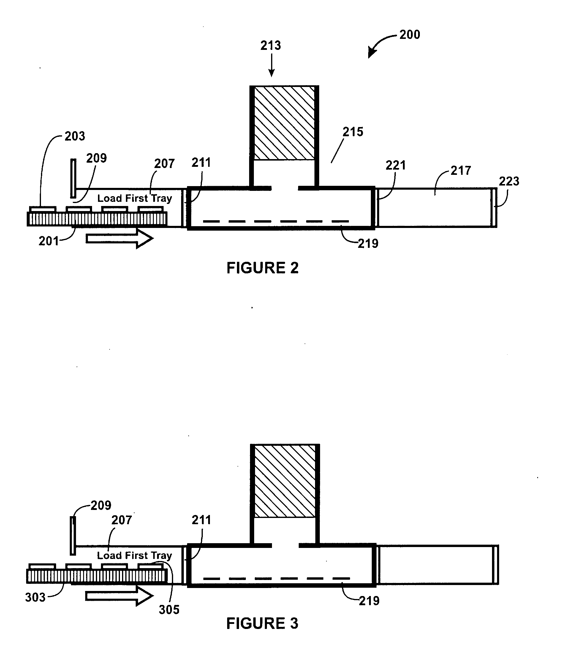
[0036] According to embodiments of the present invention, techniques including a method and a system for forming substrates using a large scale implantation process are provided. More particularly, the present method and system provide a method and system using a scanning implant process for the manufacture of substrates, for example doped substrates as may be used as photovoltaic cells. In a preferred embodiment, such implanted process provide for impurity regions in a semiconductor substrate for fabrication of photovoltaic device. The impurity region may lie in a thickness of transferable material defined by a cleave plane in a donor substrate. But it will be recognized that the invention has a wider range of applicability; it can also be applied to other types of applications such as for providing impurity regions (active regions, source / drain engineering) in three-dimensional packaging of integrated semiconductor devices, photonic devices, piezoelectronic devices, flat panel dis...


PUM


Abstract

A method for manufacturing doped substrates using a continuous large area scanning implantation process is disclosed. In one embodiment, the method includes providing a movable track member. The movable track member is provided in a chamber. The chamber includes an inlet and an outlet. In a specific embodiment, the movable track member can include one or more rollers, air bearings, belt member, and/or movable beam member to provide one or more substrates for a scanning process. The method may also include providing a first substrate. The first substrate includes a first plurality of tiles. The method maintains the first substrate including the first plurality of tiles in a vacuum. The method includes transferring the first substrate including the first plurality of tiles from the inlet port onto the movable track member. The first plurality of tiles are subjected to a scanning implant process. The method also includes maintaining a second substrate including a second plurality of tiles in the vacuum. The method includes transferring the second substrate including a second plurality of tiles from the inlet port onto the movable track member. The method includes subjecting the second plurality of tiles to an implant process using the scanning implant process.

Description

CROSS-REFERENCES TO RELATED APPLICATIONS [0001] The instant nonprovisional patent application claims priority to the following provisional patent applications, each of which is incorporated by reference in its entirety herein for all purposes: U.S. Provisional Patent Application No. 60 / 833,289 filed Jul. 25, 2006; U.S. Provisional Patent Application No. 60 / 829,147, filed Oct. 11, 2006; U.S. Provisional Patent Application No. 60 / 825,104 filed Sep. 8, 2006; and U.S. Provisional Patent Application No. 60 / 826,731 filed Sep. 22, 2006BACKGROUND OF THE INVENTION [0002] Embodiments in accordance with the present invention relate generally to techniques including methods and a structure for forming substrates, including for example doped substrates, using a large scale implantation process. More particularly, embodiments of the present method and system provides a method and system using a scanning implant process for the manufacture of photovoltaic cells. But it will be recognized that the ...

Claims


Application Information

Patent Timeline
Patent Type & Authority Applications(United States)
IPC IPC(8): H01L21/425H01L21/677
CPCH01J37/185H01J37/20H01J37/3171H01J37/32412H01L31/1804H01J2237/30H01J2237/31H01L21/67754H01J2237/184Y02E10/547Y02P70/50H01L21/67706
Inventor HENLEY, FRANCOIS J.
Owner SILICON GENERAL CORPORATION
Why Eureka
Try Eureka