Piezoelectric Component and Method for Producing It

a technology of piezoelectric components and components, applied in the direction of impedence networks, electrical equipment, etc., can solve the problems of inability to produce multi-stage filters with a ladder structure and stop band attenuation of more than 50 db in practice, the production of these types of filters is generally complicated and thus cost-intensive, and achieves the effect of low reflection impedan

Inactive Publication Date: 2008-02-28
AVAGO TECH INT SALES PTE LTD
View PDF11 Cites 22 Cited by
  • Summary
  • Abstract
  • Description
  • Claims
  • Application Information

AI Technical Summary

Benefits of technology

[0010] Therefore, the present invention is based on the object of providing piezoelectric components which significantly reduce or entirely avoid the disadvantages described above. In particular, the object of the present invention is to provide piezoelectric components which can be produced with a relatively low process outlay.

Problems solved by technology

Therefore, at the present time, multistage filters having a ladder structure and a stop band attenuation of more than 50 dB cannot be produced in practice.
However, the use of these types of filters is subject to some significant restrictions.
However, these types of filters can be miniaturized only with difficulty and their production is generally complicated and thus cost-intensive.
This makes them unsuitable for use in low price products.
Furthermore, these filter structures generally cannot be integrated into the customary processes of semiconductor fabrication.
The principle of stacked crystal filters has been known for approximately 40 years, but has been unable to gain general acceptance on an industrial scale in the MHz frequency range since the production of corresponding quartz laminae with center electrodes was not mastered.
What is common to all the stacked crystal filters described therein, however, is that their production, on account of their complex construction and the associated high number of layers to be deposited and to be patterned, requires a high process outlay which increases the production costs of the filters.

Method used


Image

  • Piezoelectric Component and Method for Producing It
  • Piezoelectric Component and Method for Producing It
  • Piezoelectric Component and Method for Producing It

Examples


Embodiment Construction

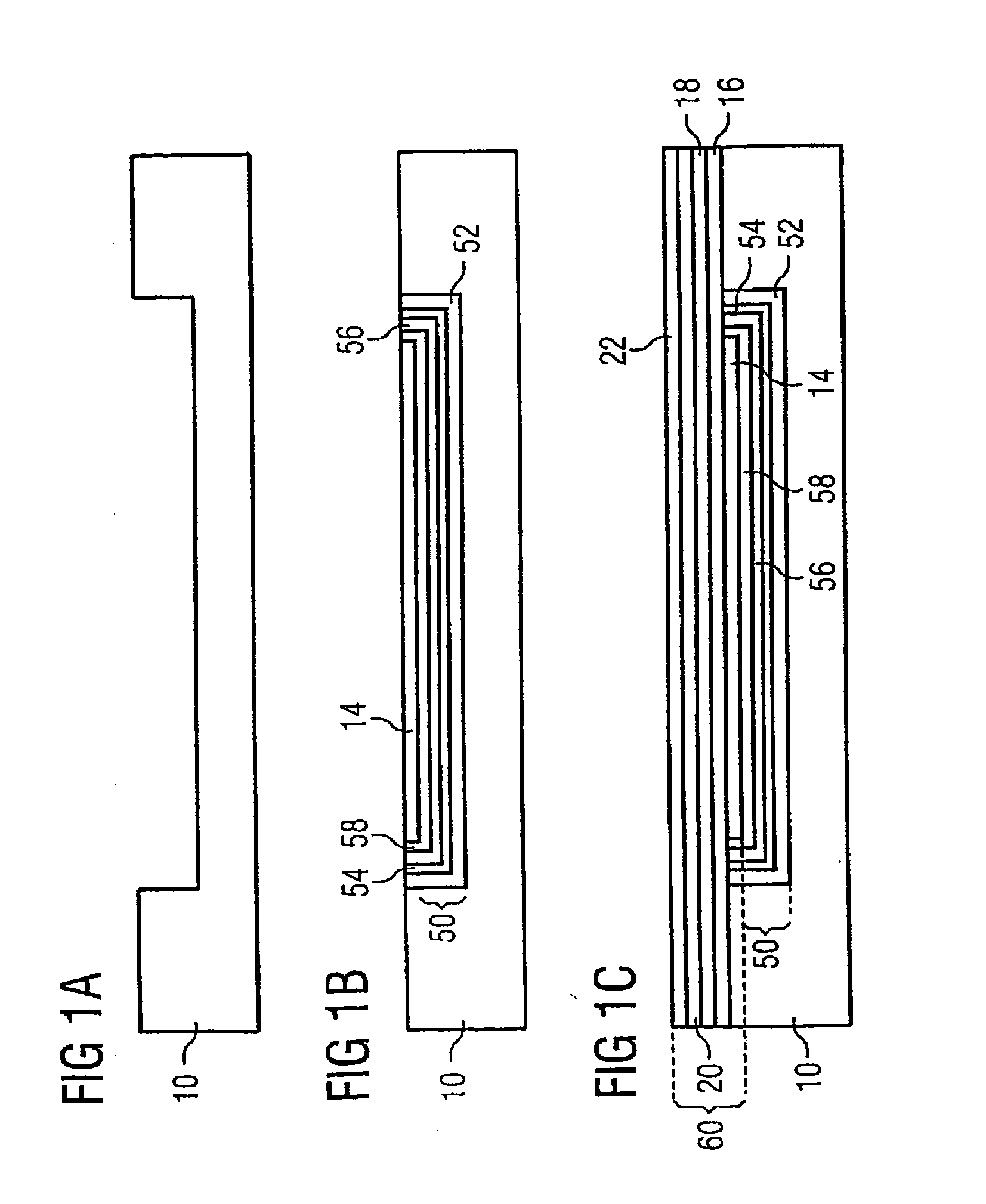
[0056]FIGS. 1A to 1E show a diagrammatic illustration of a preferred embodiment of the method according to the invention. FIG. 1A illustrates a substrate 10, in which a trench has been produced by conventional patterning techniques, e.g. lithography and etching. A layer stack is deposited in said trench, said layer stack containing the layers 52, 54, 56, 58 for producing a lower acoustic mirror 50 and a first electrically conductive layer. The bottom electrode 14 is produced from the first electrically conductive layer.

[0057] After the deposition of this layer stack, the lower acoustic mirror 50 and the bottom electrode 14 are patterned. This may be done by means of a CMP method, as is described for example in the German patent application DE 199 47 081.

[0058]FIG. 1B shows the substrate 10 with the patterned lower acoustic mirror 50 and the patterned bottom electrode 14. The first piezoelectric layer 16, the second electrically conductive layer, the second piezoelectric layer 20 a...


PUM

PropertyMeasurementUnit
piezoelectricaaaaaaaaaa
electrical potentialaaaaaaaaaa
electrically conductiveaaaaaaaaaa

Abstract

A piezoelectric component comprises at least two stacked crystal filters on a substrate. Each stacked crystal filter comprises a bottom electrode, a first piezoelectric layer arranged above the bottom electrode, a central electrode arranged above the first piezoelectric layer, a second piezoelectric layer arranged above the central electrode, and a top electrode arranged above the second piezoelectric layer. The bottom electrodes are directly connected to one another and the central electrodes are directly connected to one another.

Description

CROSS REFERENCE TO RELATED APPLICATION [0001] This application is a divisional of, and claims priority to, U.S. application Ser. No. 10 / 808,949 filed 25 Mar. 2004, the contents of which application are incorporated herein in their entirety by reference.TECHNICAL FIELD OF THE INVENTION [0002] The present invention relates to piezoelectric components comprising at least two stacked crystal filters, and to a method for producing such piezoelectric components. BACKGROUND OF THE INVENTION [0003] As mobile communication and data transmission become increasingly more widespread, there is also an ever increasing interest in the development of filters and resonators or narrowband applications with high stop band attenuation. Filters for GPS devices (global positioning system) having a 10 MHz bandwidth at 1.57 GHz or resonators for frequency standards are examples of such applications. [0004] A high stop band attenuation is usually achieved by using multistage filters in which, by way of exam...

Claims


Application Information

Patent Timeline
Patent Type & Authority Applications(United States)
IPC IPC(8): H03H9/00H03H3/04H03H3/02H03H9/58H03H9/60
CPCH03H3/04H03H9/0095H03H9/585Y10T29/42H03H9/60Y10T29/49126Y10T29/49128H03H9/589
Inventor AIGNER, ROBERTMARKSTEINER, STEPHANNESSLER, WINFRIED
Owner AVAGO TECH INT SALES PTE LTD
Why Eureka
Try Eureka