Circuit and method for generating column path control signals in semiconductor device

a technology of circuit and path control, applied in logic circuit coupling/interface arrangement, digital storage, instruments, etc., can solve problems such as erroneous read or write operation

Active Publication Date: 2008-04-17
SK HYNIX INC
View PDF13 Cites 5 Cited by
  • Summary
  • Abstract
  • Description
  • Claims
  • Application Information

AI Technical Summary

Benefits of technology

The technical effect of this patent is that it provides methods for generating column path control signals in a semiconductor device by creating multiple delayed strobe signals with specific delays and then combining them through logic operations or delaying their actions until they are needed during various stages of memory access operations. This allows for more efficient and precise control over the timing and performance of these critical functions within the semiconductor device.

Problems solved by technology

This patent discusses a technical problem related to the generation of column path control signals in a semiconductor device such as a DRAM. Due to differences in factors like process, voltage, and temperature between components used in the circuit, the timing at which these signals occur may vary, resulting in errors during read or write operations. There is thus a need for an improved solution for generating these controls.

Method used


Image

  • Circuit and method for generating column path control signals in semiconductor device
  • Circuit and method for generating column path control signals in semiconductor device
  • Circuit and method for generating column path control signals in semiconductor device

Examples


Embodiment Construction

[0030]Preferred embodiments of the present disclosure will now be described in detail with reference to the accompanying drawings.

[0031]In a column path control signal generating circuit and method according to the present disclosure, generation of column path control signals required for a read / write operation in a semiconductor device is achieved, using delay of a strobe signal through the same delay unit. Accordingly, the column path control signals can be generated under the condition in which they have been influenced by the same process, voltage, and temperature (PVT) characteristic variation of CMOS transistors. As a result, the initially-designed timing margins among the column path control signals can be maintained.

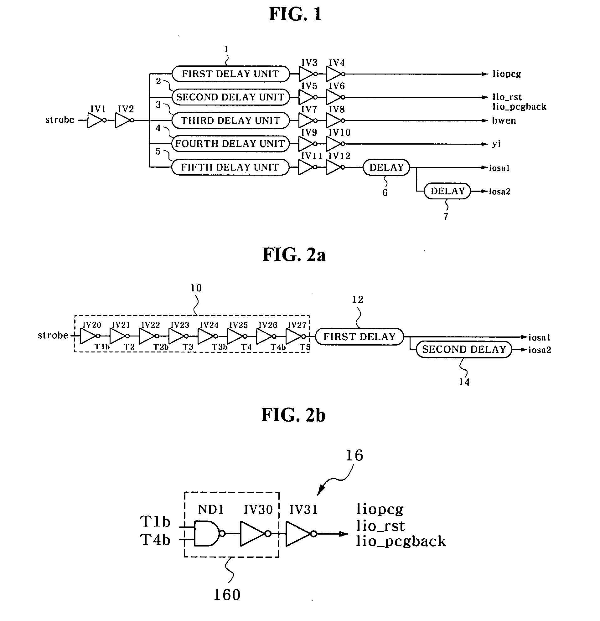
[0032]FIGS. 2A to 2C are circuit diagrams illustrating a column path control signal generating circuit according to an exemplary embodiment of the present disclosure.

[0033]As shown in FIG. 2A, the column path control signal generating circuit includes a strobe si...


PUM


Abstract

A circuit for generating column path control signals in a semiconductor device is provided. The circuit includes a strobe signal delay unit configured to receive a strobe signal, and delay the received strobe signal for different delay periods, to generate a plurality of respective delayed strobe signals, and a control signal generator configured to receive at least one of the delayed strobe signals, and perform a logical operation to the received signal, to generate a first column path control signal for controlling a column path of the semiconductor device.

Description


Claims


Application Information

Patent Timeline
Owner SK HYNIX INC
Why Eureka
Try Eureka