Programmable Leakage Test For Interconnects In Stacked Designs

a technology of interconnects and leakage tests, applied in error detection/correction, detecting faulty computer hardware, instruments, etc., can solve problems such as increasing power consumption along the way, limiting chip stacking, and affecting signal speed

Inactive Publication Date: 2014-09-04
MENTOR GRAPHICS CORP
View PDF0 Cites 5 Cited by
  • Summary
  • Abstract
  • Description
  • Claims
  • Application Information

AI Technical Summary

Problems solved by technology

However, chip stacking is limited by wiring-related problems.
Today's interconnects do not run through the silicon itself but go millimeters around it, impeding speedy signaling and increasing power consumption along the way.
Even the thinnest interconnects must still be packed along the edges of a chip, imposing strict limits on how many input / output connections the chip can handle.
But as a wafer heats up, copper expands at more than five times the rate that silicon does, exerting stress that can crack the wafer and render it useless.
Because of such imperfect etching, ragged wafer surface, and potential wafer misalignments, certain TSVs in one wafer after thinning and polishing might not be completely exposed or aligned with their counterparts on the other wafer.
Since the bonding quality of TSVs depends on the winding level of the thinned wafer as well as the surface roughness and cleanness of silicon dies, defective TSVs tend to occur in clusters, though even a single TSV defect between any two layers can void the entire chip stack, reducing the overall yield.
These mechanisms can lead to not only catastrophic defects but also parametric defects.
There are two major parametric defects occurring at TSVs, resistive open defects and leakage defects.
A resistive open defect occurs when a TSV has excessive resistance, which could result in extra delay across the TSV.
However, for more elusive small delay, conventional at-speed test is unavailable.
A leakage defect occurs when the conducting material of a TSV mistakenly penetrates the insulator between a TSV and its surrounding substrate.
Such a defect causes leakage during the time when the TSV is being charged up to a high voltage.
It could degrade the performance of the TSV and sometimes pose a reliability threat as the defect worsens over time.
First, the method is not very easy to implement.
Second, the method usually targets leakage current in the range from 10 μA to 100 μA, and may not be very suitable for the detection of small leakage (e.g., less than 1 μA), because in that case the equivalent leakage resistance would be about 100 kΩ, assuming VDD=1 V and 2 kΩ for the pull-up device 110 and resulting stable voltage at the observation node 120 would be about 0.98 V. Detection whether a voltage is greater than this value with VDD=1 V is too challenging.
However, two issues may prevent it from being applicable to the TSV leakage test directly.
As to be analyzed in detail later, this CAF-WAS method uses 2˜3 test clock cycles as the waiting time period and may not be good for handling small capacitance.

Method used


Image

  • Programmable Leakage Test For Interconnects In Stacked Designs
  • Programmable Leakage Test For Interconnects In Stacked Designs
  • Programmable Leakage Test For Interconnects In Stacked Designs

Examples


Embodiment Construction

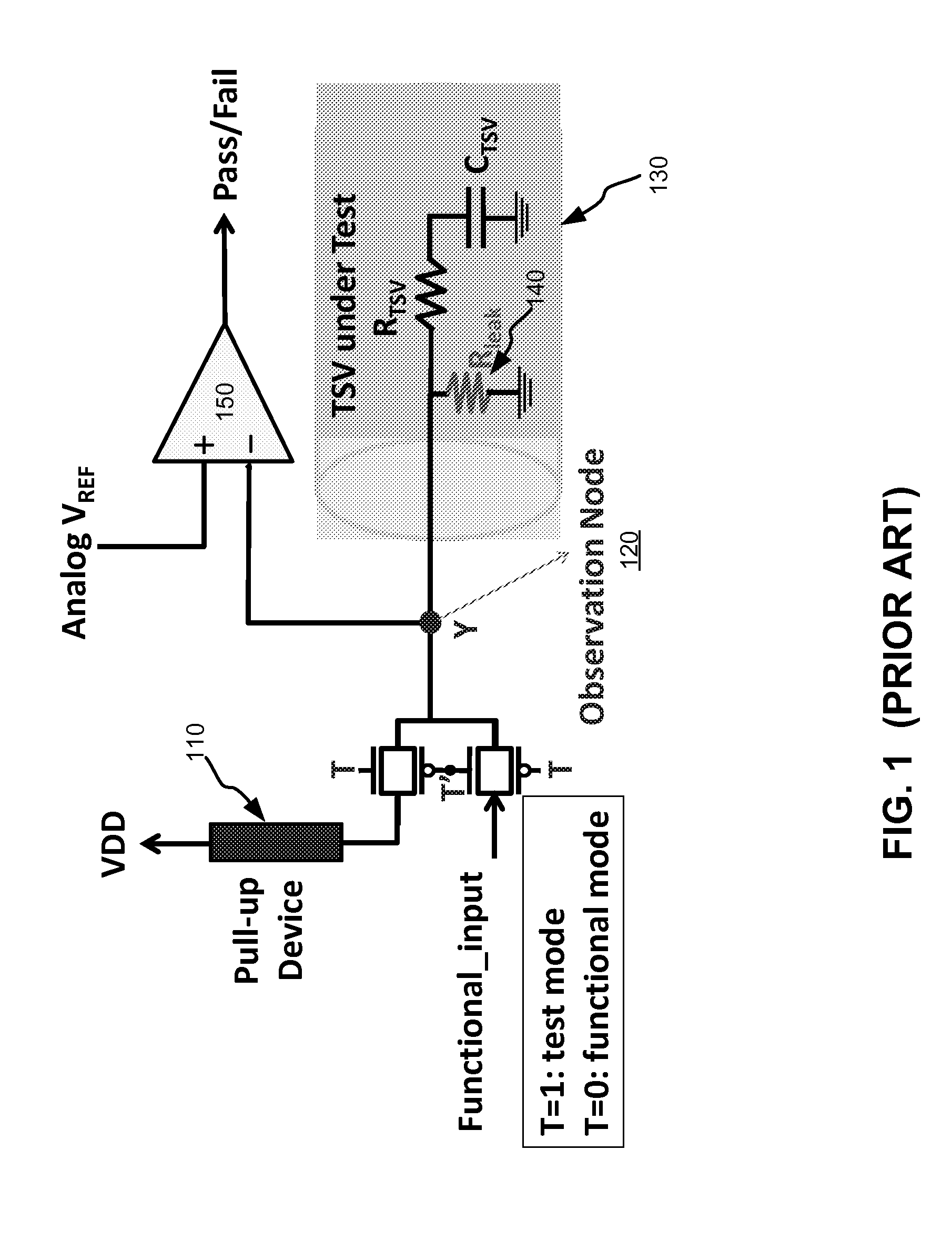
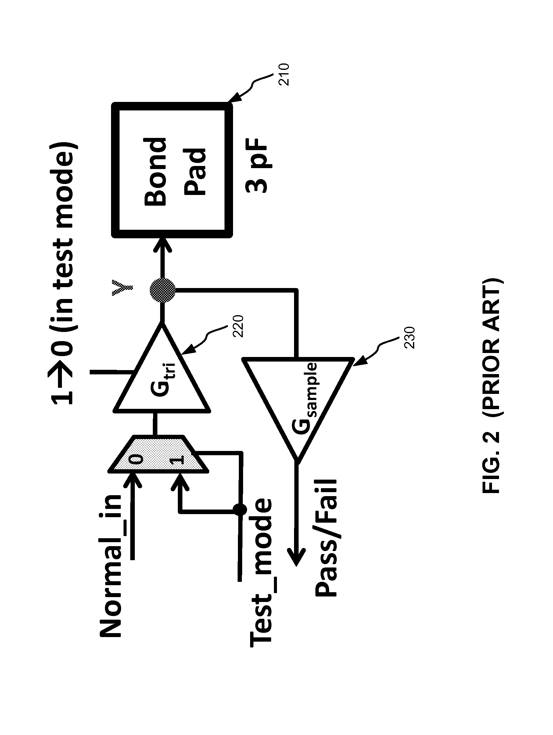
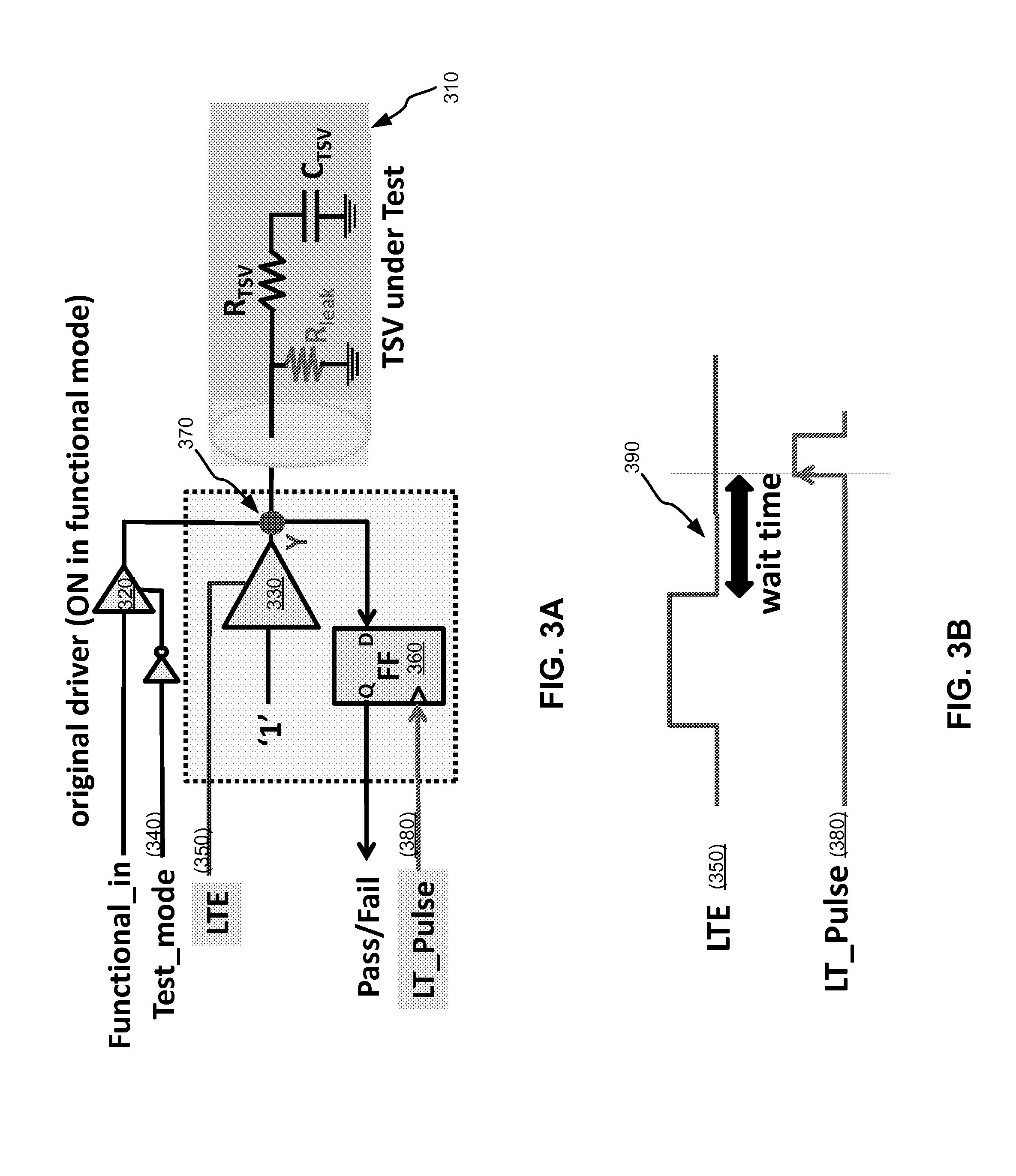
[0034]Various aspects of the present invention relate to techniques of testing interconnects in stacked designs for leakage defects. Two examples of interconnects are TSVs for three-dimensional designs and interposers for two-and-half-dimensional designs. In the following description, numerous details are set forth for the purpose of explanation. However, one of ordinary skill in the art will realize that the invention may be practiced without the use of these specific details. In other instances, well-known features have not been described in details to avoid obscuring the present invention.

[0035]Some of the techniques described herein can be implemented in software instructions stored on one or more non-transitory computer-readable media, software instructions executed on a processor, or some combination of both. As used herein, the term “non-transitory computer-readable medium” refers to computer-readable medium that are capable of storing data for future retrieval, and not propa...


PUM


Abstract

Aspects of the invention relate to techniques of testing interconnects in stacked designs for leakage defects. Logic “1” or “0” is first applied to one end of an interconnect during a first pulse. Then, logic value at the one end is captured, which triggered by an edge of a second pulse. The first pulse precedes the second pulse by a time period being selected from a plurality of delay periods. The plurality of delay periods is generated by a device shared by a plurality of interconnects.

Description

RELATED APPLICATIONS[0001]This application claims priority to U.S. Provisional Patent Application No. 61 / 771,767, filed on Mar. 1, 2013, and naming Shi-Yu Huang et al. as inventors, which application is incorporated entirely herein by reference.FIELD OF THE INVENTION[0002]The present invention relates to the field of integrated circuit (IC) testing technology. Various implementations of the invention may be particularly useful for testing and characterizing interconnects of stacked integrated circuits.BACKGROUND OF THE INVENTION[0003]Expanding into the third dimension enables chip manufacturers to continue shrinking transistors to boost speed without adding power leaks. However, chip stacking is limited by wiring-related problems. Today's interconnects do not run through the silicon itself but go millimeters around it, impeding speedy signaling and increasing power consumption along the way. 2-D (horizontal) real estate is also valuable. Even the thinnest interconnects must still be...

Claims


Application Information

Patent Timeline
Patent Type & Authority Applications(United States)
IPC IPC(8): G06F17/50
CPCG06F17/5081G01R31/31715G01R31/318513G11C29/025G11C2029/5006
Inventor HUANG, SHI-YUTSAI, KUN-HANCHENG, WU-TUNGLIN, YU-HSIANGHUANG, LI-REN
Owner MENTOR GRAPHICS CORP
Why Eureka
Try Eureka