Etching method

a technology of etching and etching layers, applied in the direction of basic electric elements, semiconductor/solid-state device manufacturing, electric devices, etc., can solve the problems of increasing the difficulty and cost of high-resolution lithography techniques, the cd of the corresponding opening in the etching layer cannot meet the requirement, and the dimension of the semiconductor device unceasingly gets smaller, so as to reduce the after-etching inspection. effect of inspection

Inactive Publication Date: 2008-04-17
UNITED MICROELECTRONICS CORP
View PDF2 Cites 2 Cited by
  • Summary
  • Abstract
  • Description
  • Claims
  • Application Information

AI Technical Summary

Benefits of technology

[0007] In view of the foregoing, this invention provides an etching method that is capable of reducing the after-etching-inspection (AEI) CD.
[0008] Another object of this invention is to provide an etching method that is capable of reducing the critical dimension of patterns to increase the integration degree of IC.
[0009] Still another object of this invention is to provide a method for forming a contact opening, which is capable of preventing bridging between adjacent contact plugs to improve the reliability of semiconductor devices.
[0024] The etching method of this invention is capable of forming a protective layer on the top surface of the patterned photoresist layer and a spacer on the sidewall of the same, so that the photoresist loss in the etching steps can be reduced, and the opening expansion problem can be avoid so that the after-etching-inspection (AEI) CD is smaller than the after-development-inspection (ADI) CD. Therefore, the CD of the devices can be reduced effectively. It is particularly noted that adopting the etching method of this invention can also improve the etching selectivity effectively.
[0025] Since the method for forming a contact opening of this invention can prevent the opening expansion effect, adjacent contact openings will not overlap with each other to cause bridging between adjacent contact plugs. Therefore, the reliability of the devices can be improved.

Problems solved by technology

As the integration degree of IC is always required to be higher, the dimension of semiconductor devices unceasingly gets smaller.
However, high-resolution lithography techniques are more difficult and expensive due to the limitations of optics.
However, since an opening in the photoresist layer and the anti-reflection coating (ARC) is easily expanded in such an etching method, the CD of the corresponding opening in the etched layer cannot meet the requirement.
On the other hand, the above etching method has a limitation on the extent of CD reduction and may cause a striation effect, upon which the top-view profile of the openings is much changed so that adjacent openings overlap with each other to cause bridging between adjacent contact plugs.
Therefore, the reliability of the devices is lowered.

Method used


Image

  • Etching method
  • Etching method
  • Etching method

Examples


Embodiment Construction

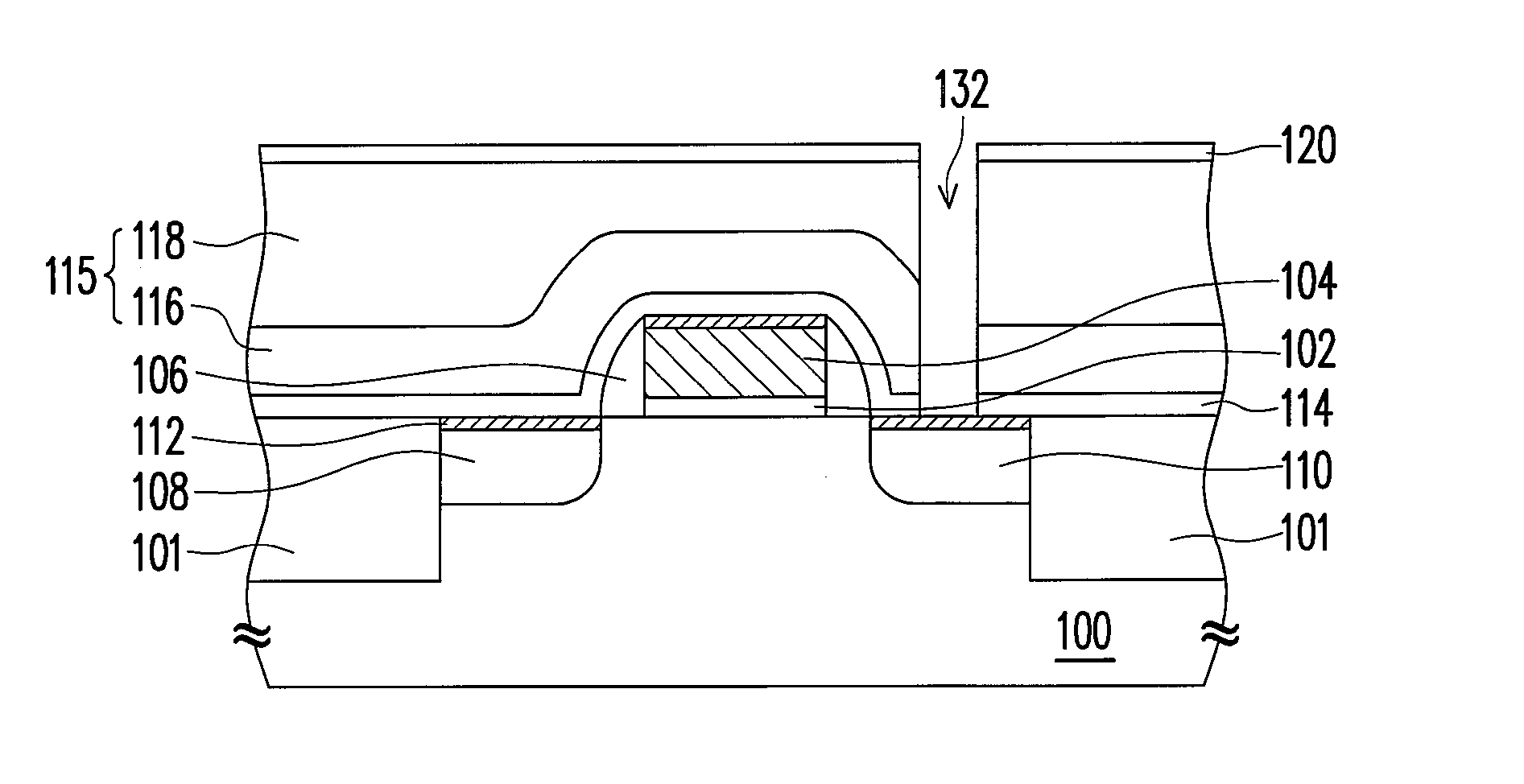
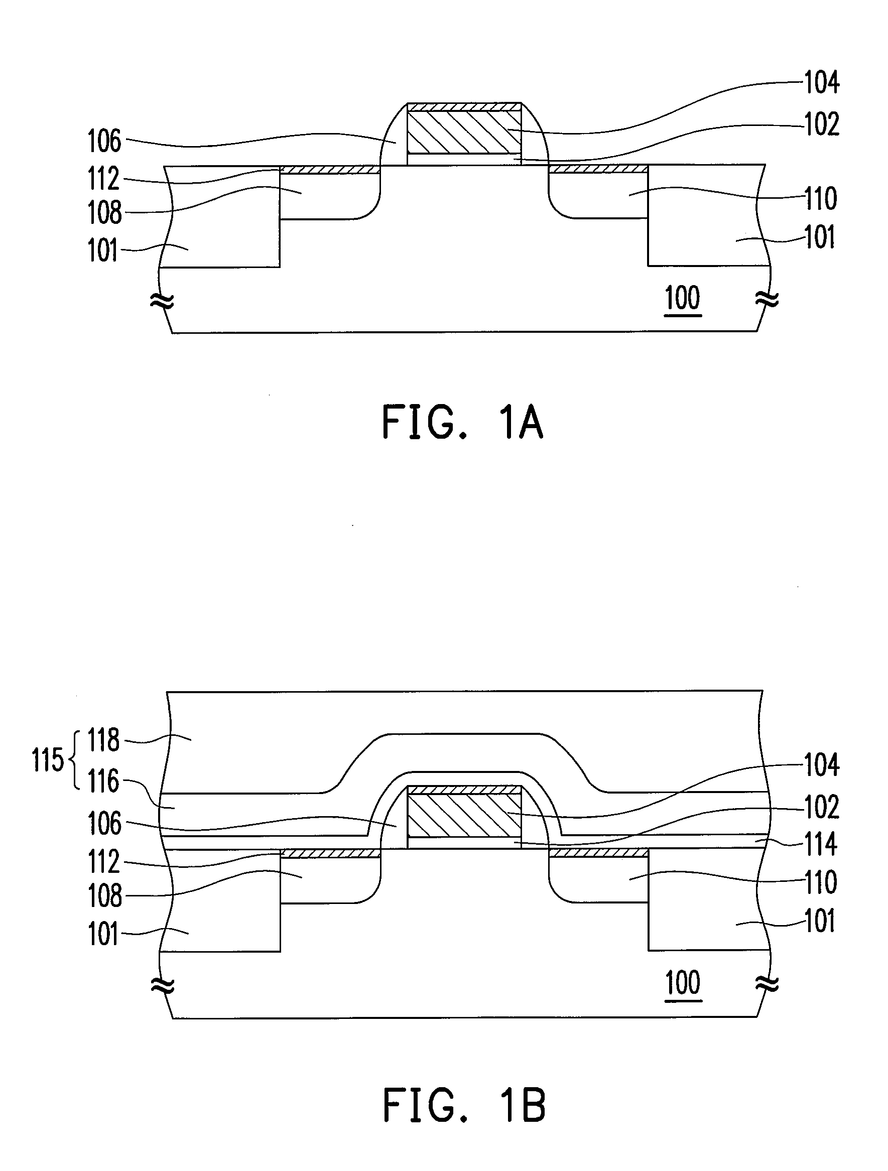
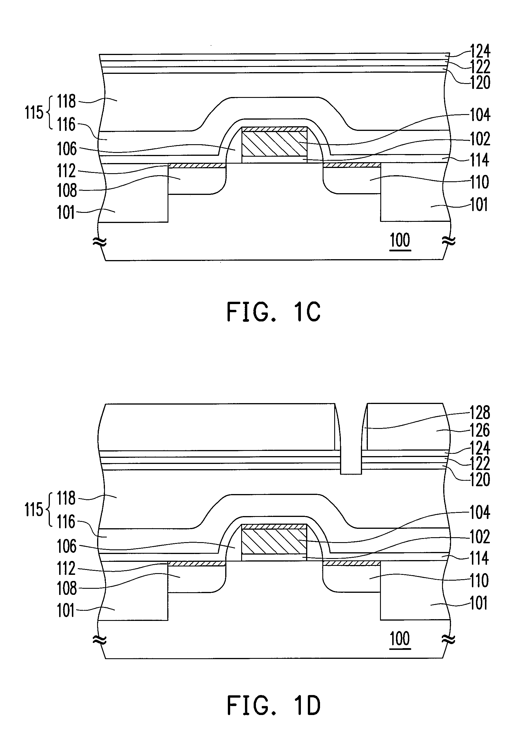
[0028] Referring to FIG. 1A, a semiconductor substrate 100 having a metal-oxide-semiconductor (MOS) device thereon is provided, wherein the MOS device is isolated from adjacent devices by an isolation structure 110 like a shallow-trench-isolation (STI) structure. In the MOS device, a gate 104 is formed on a gate dielectric layer 102, and a spacer 106 is formed on the sidewall of the gate 104. A source region 108 and a drain region 110 are formed in the substrate 100 beside the gate 104. In another embodiment, a metal silicide layer 112 is further formed on the gate 104, the source region 108 and the drain region 110 to reduce their resistance, wherein the material of the metal silicide layer 112 may be nickel silicide, tungsten silicide or cobalt silicide, etc. Because the material and forming method of each part in the above MOS device are known to one of ordinary skills, the description of them is omitted here.

[0029] Referring to FIG. 1B, a dielectric layer 115 is formed on the s...


PUM


Abstract

An etching method is described, including a first etching step that uses a first etching gas including a first fluorinated hydrocarbon compound, and a second etching step that uses a second etching gas including a second fluorinated hydrocarbon compound. The hydrogen content in the first fluorinated hydrocarbon compound is lower than that in the second fluorinated hydrocarbon compound, such that the after-etching-inspection (AEI) critical dimension is smaller than the after-development-inspection (ADI) critical dimension.

Description

CROSS-REFERENCE TO RELATED APPLICATION [0001] This application is a divisional of an application Ser. No. 11 / 160,131, filed on Jun. 10, 2005, now pending. The entirety of each of the above-mentioned patent applications is hereby incorporated by reference herein and made a part of this specification.BACKGROUND OF THE INVENTION [0002] 1. Field of the Invention [0003] The present invention relates to an etching method. More particularly, the present invention relates to an etching method capable of reducing critical dimension (CD), and to a method for forming a contact opening that utilizes the etching method. [0004] 2. Description of the Related Art[0005] As the integration degree of IC is always required to be higher, the dimension of semiconductor devices unceasingly gets smaller. In the prior art, the miniaturization of pattern pitch in IC fabrication is mostly made by enhancing the lithographic resolution. However, high-resolution lithography techniques are more difficult and expe...

Claims


Application Information

Patent Timeline
Patent Type & Authority Applications(United States)
IPC IPC(8): H01L21/311
CPCH01L21/31116H01L21/31144H01L21/76834H01L21/76816H01L21/32135
Inventor CHOU, PEI-YULIAO, JIUNN-HSIUNG
Owner UNITED MICROELECTRONICS CORP
Why Eureka
Try Eureka