Etch process for CD reduction of arc material

a technology of arc material and etching process, which is applied in the direction of basic electric elements, semiconductor/solid-state device manufacturing, electric apparatus, etc., can solve the problems of reducing the critical dimension of ic, requiring expensive new equipment, and limiting the smallness of ic critical dimensions. , to achieve the effect of reducing the critical dimension

Inactive Publication Date: 2006-10-05
GLOBALFOUNDRIES INC
View PDF22 Cites 13 Cited by
  • Summary
  • Abstract
  • Description
  • Claims
  • Application Information

AI Technical Summary

Benefits of technology

[0009] Another exemplary embodiment relates to a method of fabricating an integrated circuit. The method includes providing an organic anti-reflective coating, and plasma dry etching the anti-reflective coating in accordance with a feature. The feature defines a spacing. The plasma dry etching includes providing a polymerizing agent. The spacing in the anti-reflective coating has a reduced critical dimension.

Problems solved by technology

One limitation to the smallness of IC critical dimensions is conventional lithography.
Such improvements can be time consuming and expensive, often requiring expensive new equipment.
Even if a lithographic improvement is possible, a lithographic CD shrink is often accompanied by a rise in defect densities.
Generally, the ARC (organic or inorganic) layer is a relatively thin layer which is not used as a hard mask because it is too thin and does not allow thickness flexibility due to optical design parameters.
Conventional spacer etching processes generally have not been used with organic ARC layers due to material incompatibility issues associated with oxide and nitride spacer processes.
Thus, there is a need to shrink CD features using non-conventional polymerizing etch techniques.

Method used


Image

  • Etch process for CD reduction of arc material
  • Etch process for CD reduction of arc material
  • Etch process for CD reduction of arc material

Examples


Embodiment Construction

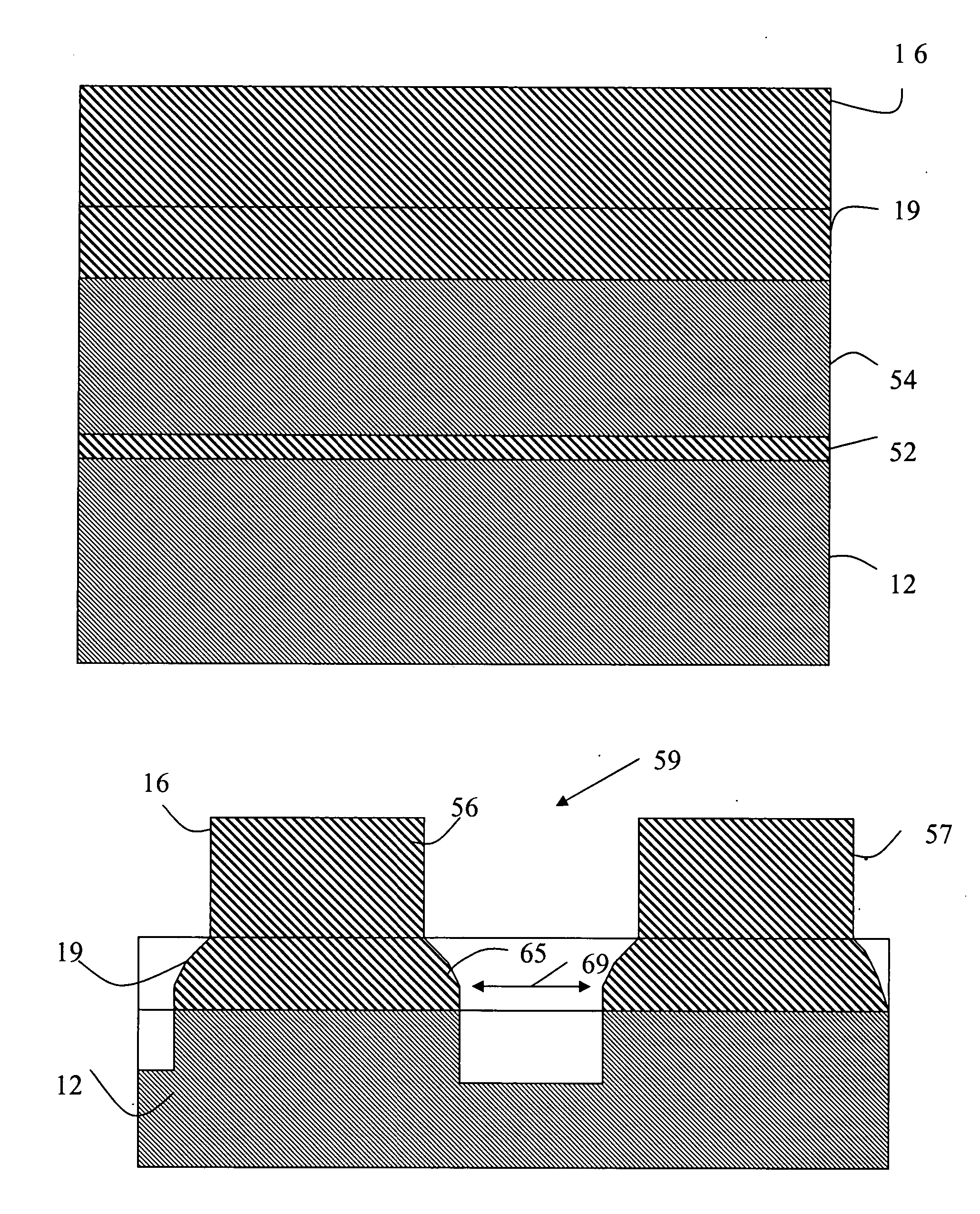
[0022] Referring to FIG. 1, a substrate 12 is shown in an etching system 10. Substrate 12 can be a semiconductor substrate, such as, silicon, gallium arsenide, germanium, or other substrate material. Substrate 12 can include one or more layers of material thereon. The layers can be insulative layers, conductive layers, barrier layers, or other layers of material which are to be etched, or selectively removed using the process described herein.

[0023] Substrate 12 can include one or more layers of material and / or features, such as, lines, interconnects, vias, doped portions, etc., and can further include devices, such as, transistors, microactuators, microsensors, capacitors, resistors, diodes, etc. Substrate 12 can be an entire IC wafer or part of an IC wafer. Substrate 12 can be part of an integrated circuit, such as, a memory, a processing unit, an input / output device, etc.

[0024] Etching system 10 is preferably a dry etching system for forming features on substrate 12 or layers a...


PUM


Abstract

A method of reducing critical dimensions of a feature in a anti-reflective coating layer structure can utilize a polymerizing agent. The anti-reflective coating structure can be utilized to form various integrated circuit structures. The anti-reflective coating can be utilized to form gate stacks comprised of polysilicon and a dielectric layer, conductive lines, or other IC structure. The polymerizing agent can include carbon, hydrogen and fluorine.

Description

FIELD OF THE INVENTION [0001] The present specification relates to the fabrication of integrated circuits (ICs). More specifically, the present specification relates to a critical dimension (CD) reduction process for forming integrated circuit features. BACKGROUND OF THE INVENTION [0002] Semiconductor devices or integrated circuits (ICs) can include millions of devices, such as, transistors. Ultra-large scale integrated (ULSI) circuits can include complementary metal oxide semiconductor (CMOS) field effect transistors (FET). Despite the ability of conventional systems and processes to fabricate millions of devices on an IC, there is still a need to decrease the size of IC device features, and, thus, increase the number of devices on an IC. [0003] One limitation to the smallness of IC critical dimensions is conventional lithography. In general, projection lithography refers to processes for pattern transfer between various media. According to conventional projection lithography, a si...

Claims


Application Information

Patent Timeline
Patent Type & Authority Applications(United States)
IPC IPC(8): H01L21/4763
CPCH01L21/3088H01L21/32139H01L21/31144H01L21/0338H01L21/0276
Inventor JONES, PHILLIP L.CHANG, MARK S.BELL, SCOTT A.
Owner GLOBALFOUNDRIES INC
Why Eureka
Try Eureka