Etch pattern definition using a CVD organic layer as an anti-reflection coating and hardmask

a technology of organic layer and anti-reflection coating, which is applied in the direction of electrical equipment, decorative arts, and semiconductor devices, can solve the problems of adversely affecting resolution and limited thickness of a given photoresist layer, and achieve the effect of effectively trimming, high-effective hard mask properties, and improving pattern resolution

Inactive Publication Date: 2008-08-21
APPLIED MATERIALS INC
View PDF12 Cites 14 Cited by
  • Summary
  • Abstract
  • Description
  • Claims
  • Application Information

AI Technical Summary

Benefits of technology

[0017]One advantage of the present invention is that a structure is provided, which has both antireflective properties and highly effective hard mask properties.
[0018]Another advantage of the present invention is that masking structure is provided whose formation requires only a very thin photoresist layer, thus improving pattern resolution.
[0019]Another advantage of the present invention is that a masking structure is provided that can be effectively trimmed to decrease the critical dimensions of the features being etched.
[0020]Another advantage is that the CVD organic layer can be trimmed with a dielectric antireflective coating (DARC) or thin silicon oxide layer as the mask to achieve smaller critical dimensions of the features being etched.
[0021]Yet another advantage of the present invention is that a masking structure is provided that can easily be removed.
[0022]The above and other embodiments and advantages of the present invention will become apparent to those of ordinary skill in the art upon reading the detailed description and claims to follow.

Problems solved by technology

Unfortunately, the thickness of a given photoresist layer is frequently limited by the thickness of the material that is to be etched and the selectivity that exists between the photoresist and the material that is to be etched.
These standing waves can cause, for example, sinusoidal undulations at the edges of the photoresist features that are produced, adversely affecting resolution.

Method used


Image

  • Etch pattern definition using a CVD organic layer as an anti-reflection coating and hardmask
  • Etch pattern definition using a CVD organic layer as an anti-reflection coating and hardmask
  • Etch pattern definition using a CVD organic layer as an anti-reflection coating and hardmask

Examples


Embodiment Construction

[0027]As a preface to the detailed description, it should be noted that, all percentages (%) listed for gas constituents are % by volume, and all ratios listed for gas constituents are volume ratios.

[0028]The term “selectivity” is used to refer to a) a ratio of etch rates of two or more materials and b) a condition achieved during etch when etch rate of one material is increased in comparison with another material.

[0029]The present invention now will be described more fully hereinafter with reference to the accompanying drawings, in which preferred embodiments of the present invention are shown. This invention may, however, be embodied in different forms and should not be construed as limited to the embodiments set forth herein.

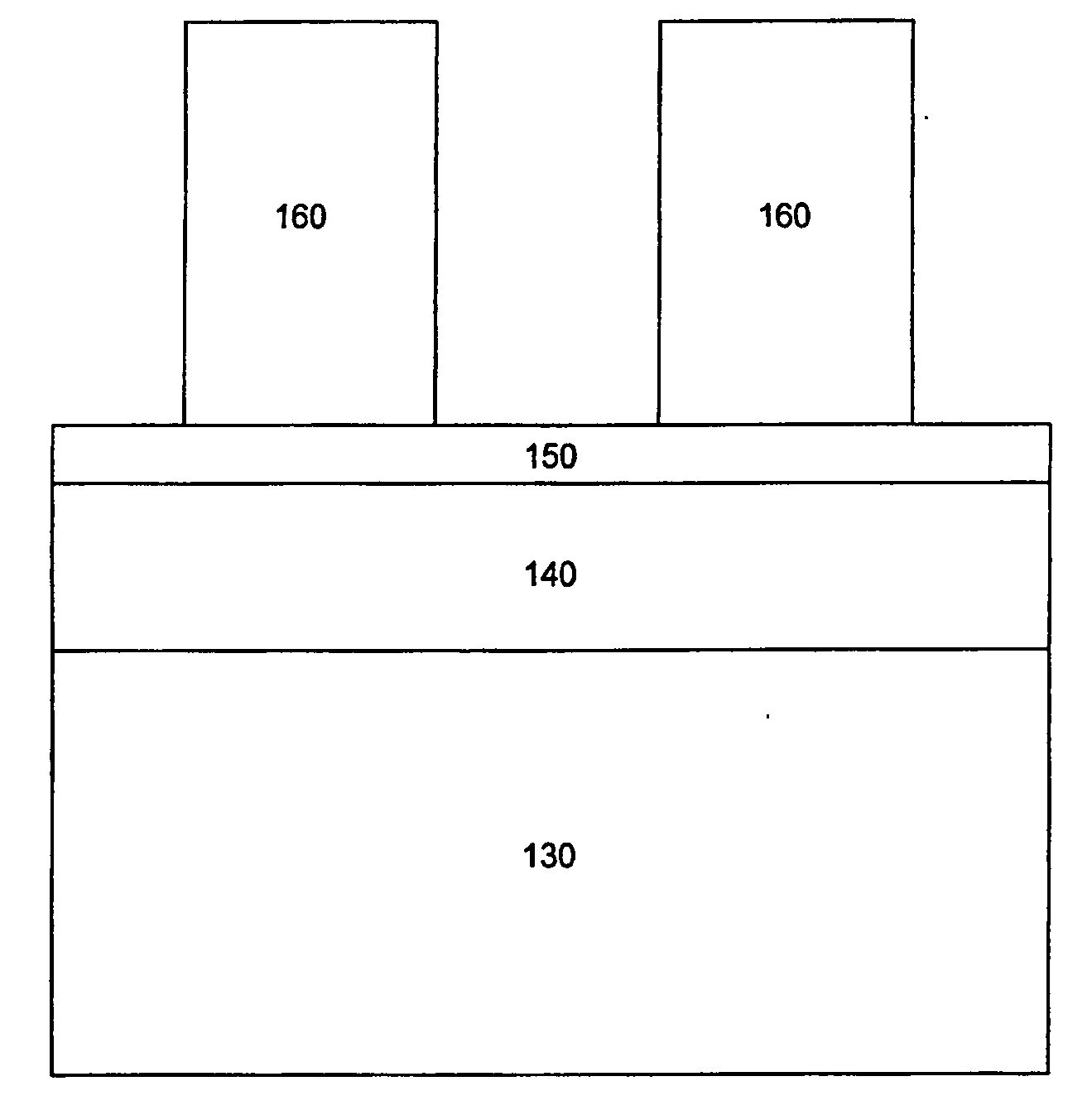
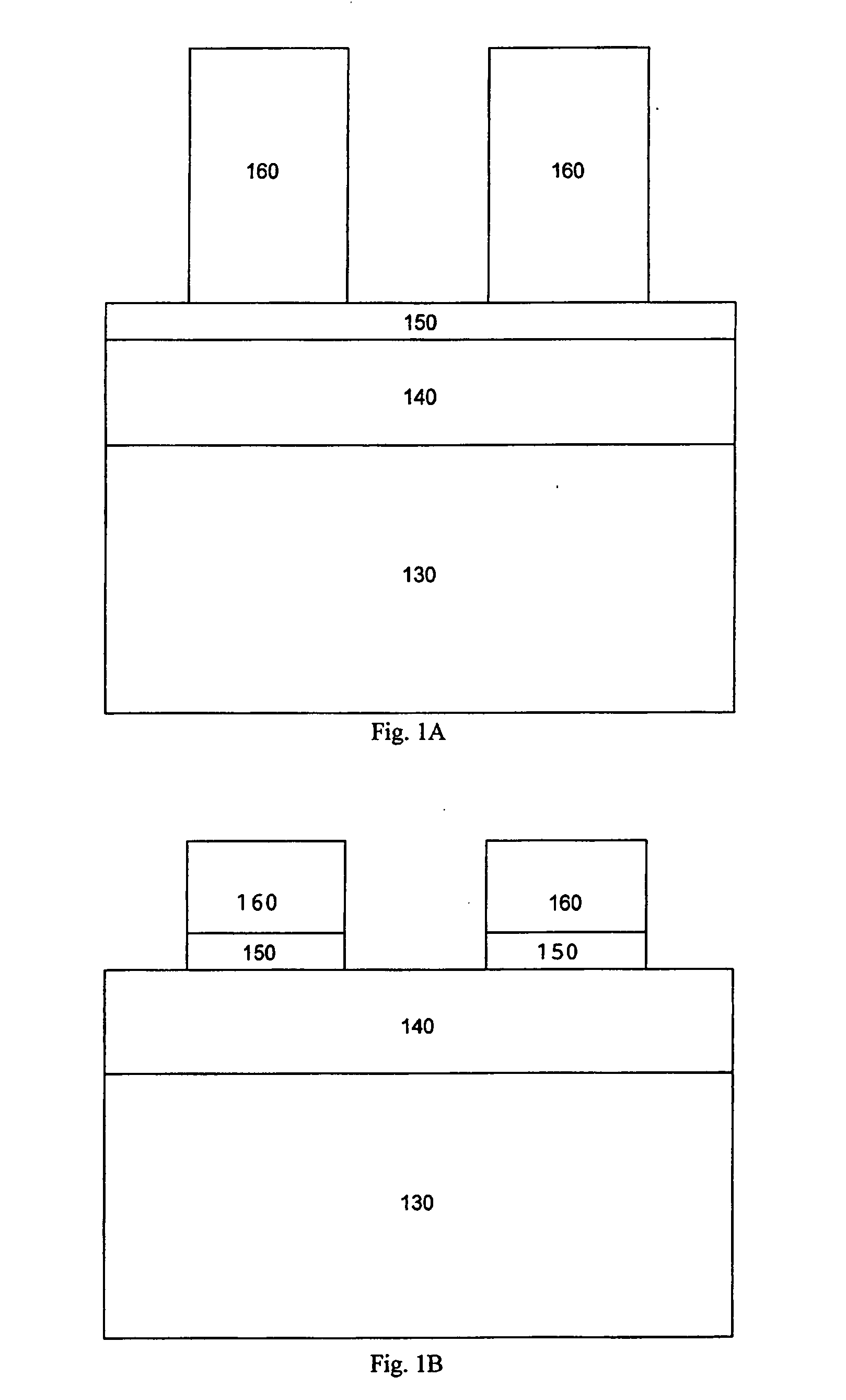
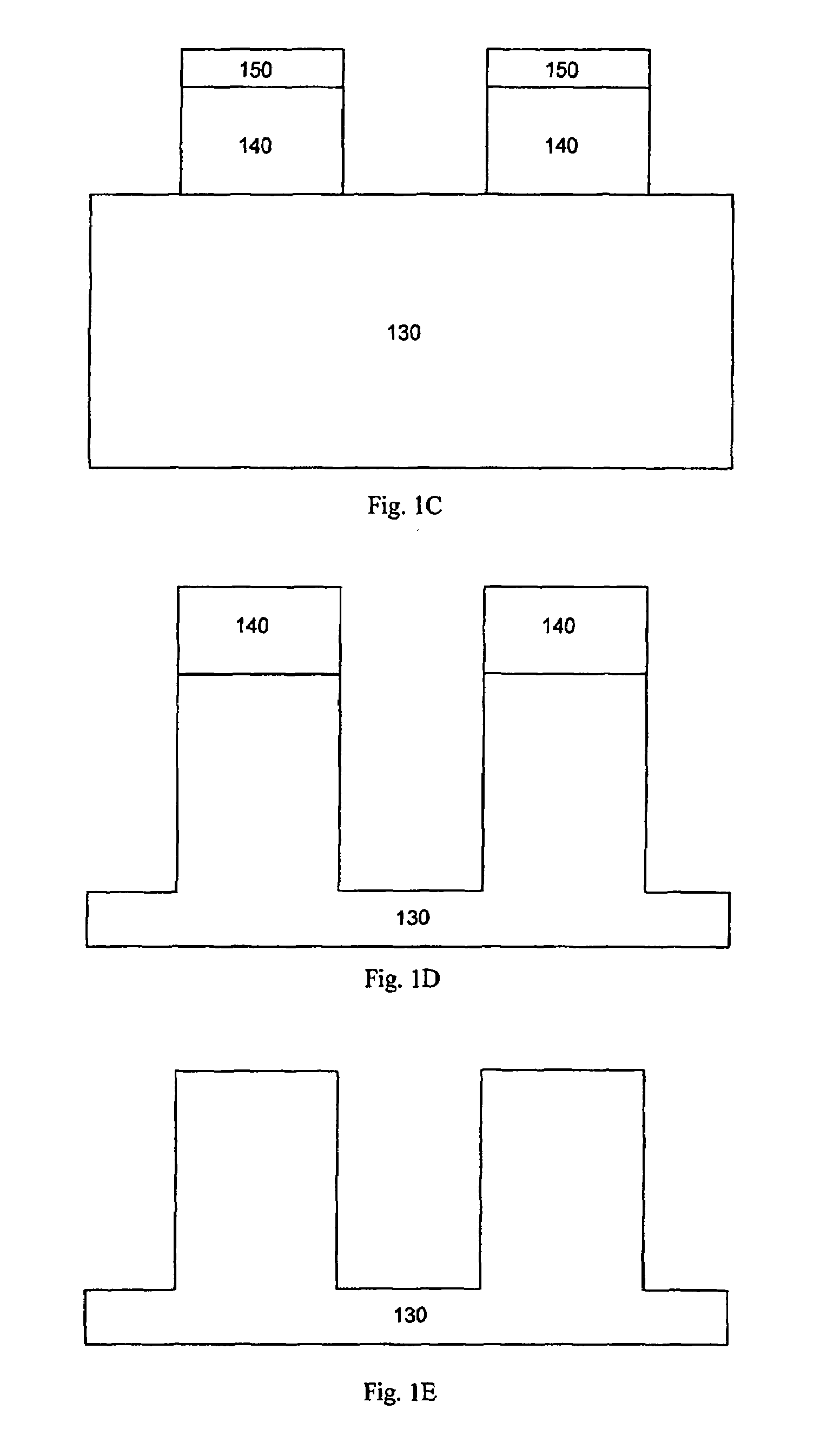
[0030]An embodiment of the present invention will now be described in connection with FIGS. 1A-1E. The multilayer structure illustrated in FIG. 1A includes a layer of material 130 to be etched, a chemical vapor deposited (CVD) organic layer 140, a dielectric ...


PUM

PropertyMeasurementUnit
refractive indexaaaaaaaaaa
thicknessesaaaaaaaaaa

Abstract

A multilayer antireflective hard mask structure is disclosed. The structure comprises: (a) a CVD organic layer, wherein the CVD organic layer comprises carbon and hydrogen; and (b) a dielectric layer over the CVD organic layer. The dielectric layer is preferably a silicon oxynitride layer, while the CVD organic layer preferably comprises 70-80% carbon, 10-20% hydrogen and 5-15% nitrogen. Also disclosed are methods of forming and trimming such a multilayer antireflective hard mask structure. Further disclosed are methods of etching a substrate structure using a mask structure that contains a CVD organic layer and optionally has a dielectric layer over the CVD organic layer.

Description

STATEMENT OF RELATED APPLICATIONS[0001]This application is a continuation of U.S. patent application Ser. No. 09 / 905,172, filed Jul. 13, 2001, entitled “Etch Pattern Definition Using A CVD Organic Layer As An Anti-Reflection Coating and Hardmask,” which is incorporated by reference in its entirety herein.BACKGROUND OF THE INVENTION[0002]1. Field of the Invention[0003]The present invention relates to anti-reflection coatings and hard masks for use in defining etch patterns within an underlying substrate structure.[0004]2. Brief Description of the Background Art[0005]Integrated circuit manufacturing processes often involve the creation of etch patterns in various materials by selective etching. For example, trenches are often made in a substrate such as silicon to provide isolation between individual devices or to provide capacitive charge storage or to define the gate for a transistor.[0006]Usually these etch patterns are created by providing a mask upon the material within which the...

Claims


Application Information

Patent Timeline
Patent Type & Authority Applications(United States)
IPC IPC(8): C23F1/00H01L21/027H01L21/28H01L21/308H01L21/311H01L21/314H01L21/3213
CPCH01L21/0276H01L21/28035H01L21/3081H01L21/32139H01L21/31138H01L21/3146H01L21/32137H01L21/3088H01L21/02115
Inventor MUI, DAVID S.LIU, WEILILL, THORSTENBENCHER, CHRISTOPHER DENNISWANG, YUXIANG MAY
Owner APPLIED MATERIALS INC
Why Eureka
Try Eureka