De-fluoridation process

a technology of defluoridation and process, which is applied in the direction of coating, chemical vapor deposition coating, decorative arts, etc., can solve the problems of unreliable features, additional problems, and short wavelength photoresists used in the field of defluoridation,

Inactive Publication Date: 2008-04-10
LAM RES CORP
View PDF46 Cites 14 Cited by
  • Summary
  • Abstract
  • Description
  • Claims
  • Application Information

AI Technical Summary

Benefits of technology

[0010]To achieve the foregoing and in accordance with the purpose of the present invention a method for forming a feature in a layer is provided. A photoresist layer is formed over the layer. The photoresist layer is patterned to form photoresist features with photoresist sidewalls, where the photoresist features have a first critical dimension. A fluorine-containing conformal layer is deposited over the sidewalls of the photoresist features to reduce the critical dimensions of the photoresist features. The fluorine contained in the conformal layer is removed, while the remaining material is left in place. Features are etched into the layer, wherein the layer features have a second critical dimension, which is less than the first critical dimension.

Problems solved by technology

Such tapering may provide unreliable features.
The use of shorter wavelength photoresists may provide additional problems over photoresists using longer wavelengths.

Method used


Image

  • De-fluoridation process
  • De-fluoridation process
  • De-fluoridation process

Examples


example recipe

[0077

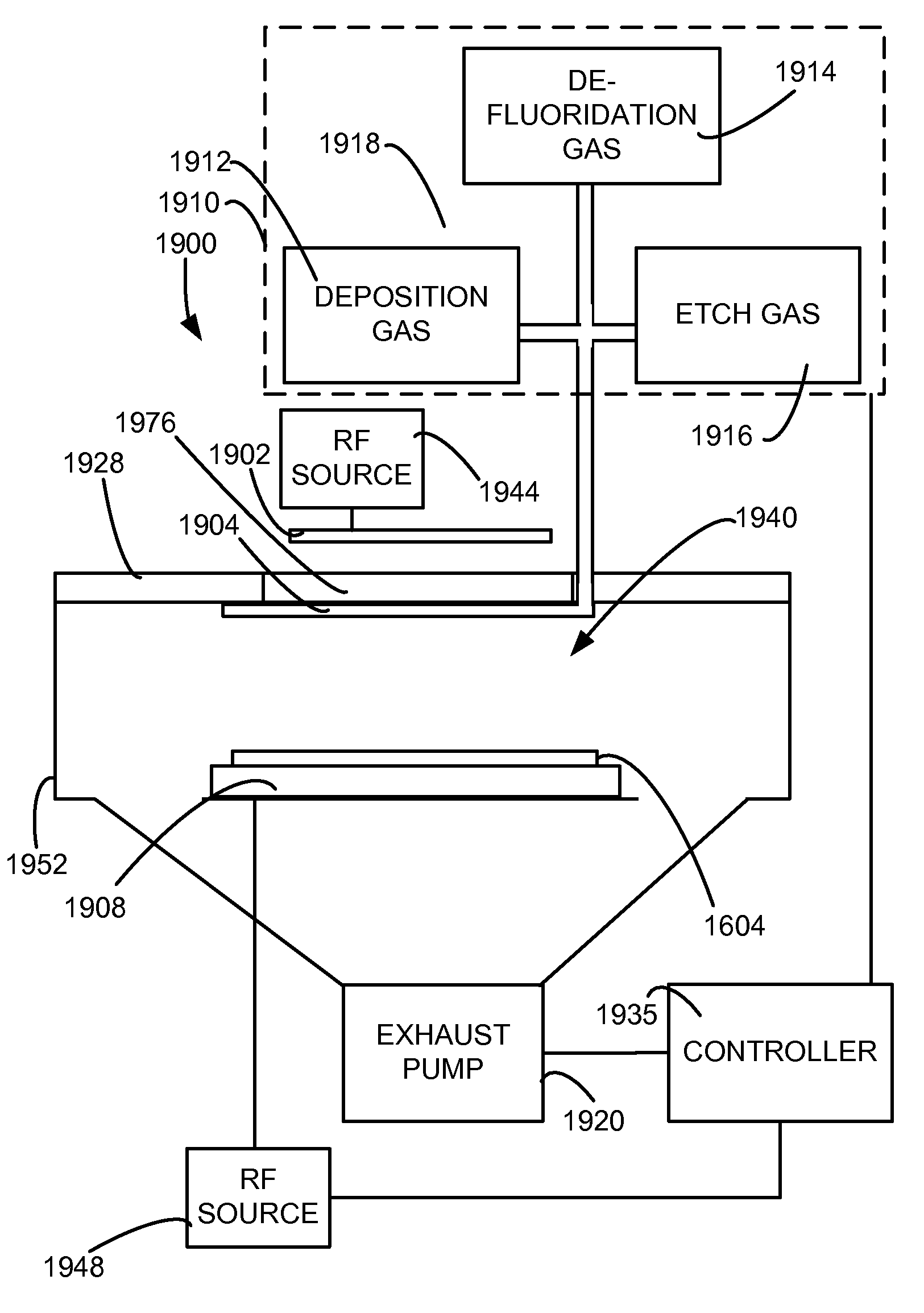
[0078]In an example recipe, a device that may be used for both depositing and etching the deposition layer and the conductive layer is the 2300 Versys™ made by LAM Research Corporation™ of Fremont, Calif. FIG. 13 is a schematic illustration of such a device 1900 used for both depositing and etching the deposition layer. The plasma processing chamber 1900 comprises an inductive antenna (or coil) 1902, a gas distribution plate (GDP) 1904, a substrate support 1908, a gas source 1910, and an exhaust pump 1920. The gas source 1910 is in fluid connection with the gas distribution plate 1904 and comprises a deposition gas source 1912, a de-fluoridation gas 1914, and an etch gas source 1916. The gas source 1910 may comprise additional gas sources, such as a second etching or deposition gas source. Within plasma processing chamber 1900, the substrate 1604 is positioned upon the substrate support 1908. The substrate support 1908 incorporates a suitable substrate chucking mechanism (e.g.,...


PUM

PropertyMeasurementUnit
angleaaaaaaaaaa
pressureaaaaaaaaaa
temperatureaaaaaaaaaa

Abstract

A feature in a layer is provided. A photoresist layer is formed over the layer. The photoresist layer is patterned to form photoresist features with photoresist sidewalls, where the photoresist features have a first critical dimension. A fluorine-containing conformal layer is deposited over the sidewalls of the photoresist features to reduce the critical dimensions of the photoresist features. Fluorine is removed from the conformal layer, while the remaining conformal layer is left in place. Features are etched into the layer, wherein the layer features have a second critical dimension, which is less than the first critical dimension.

Description

CROSS-REFERENCE TO RELATED APPLICATION[0001]This application is a divisional of and claims priority under 35 U.S.C. § 120 to commonly owned and co-pending U.S. application Ser. No. 11 / 545,903, entitled “DE-FLUORIDATION PROCESS,” filed on Oct. 10, 2006, which is incorporated herein by reference in its entirety and for all purposes.BACKGROUND OF THE INVENTION[0002]The present invention relates to the formation of semiconductor devices.[0003]During semiconductor wafer processing, features of the semiconductor device are defined in the wafer using well-known patterning and etching processes. In these processes, a photoresist (PR) material is deposited on the wafer and then is exposed to light filtered by a reticle. The reticle is generally a glass plate that is patterned with exemplary feature geometries that block light from propagating through the reticle.[0004]After passing through the reticle, the light contacts the surface of the photoresist material. The light changes the chemical...

Claims


Application Information

Patent Timeline
Patent Type & Authority Applications(United States)
IPC IPC(8): H01L21/306
CPCH01L21/0212H01L21/02274H01L21/0234H01L21/0271H01L21/0337H01L21/76816H01L21/31058H01L21/31138H01L21/3127H01L21/32139H01L21/0338H01L21/0274H01L21/67069
Inventor HEO, DONGHOKIM, JISOOSADJADI, S.M. REZA
Owner LAM RES CORP
Why Eureka
Try Eureka