Reducing gate CD bias in CMOS processing

a technology of cmos and gate cd, applied in the field of semiconductor fabrication, can solve problems such as the increase of transistor eo

Active Publication Date: 2009-07-02
TEXAS INSTR INC
View PDF11 Cites 12 Cited by
  • Summary
  • Abstract
  • Description
  • Claims
  • Application Information

AI Technical Summary

Benefits of technology

[0008]The present invention relates to forming an integrated circuit having NMOS and PMOS transistors, wherein a critical dimension (CD) bias between the NMOS and PMOS is eliminated or at least substantially reduced.

Problems solved by technology

If the dopant does not diffuse all the way down to the underlying dielectric interface, a poly depletion effect occurs, which results in an increase in the transistor EOT.

Method used


Image

  • Reducing gate CD bias in CMOS processing
  • Reducing gate CD bias in CMOS processing
  • Reducing gate CD bias in CMOS processing

Examples


Embodiment Construction

[0019]One or more aspects of the present invention are described with reference 30 to the drawings, wherein like reference numerals are generally utilized to refer to like elements throughout, and wherein the various structures are not necessarily drawn to scale. In the following description, for purposes of explanation, numerous specific details are set forth in order to provide a thorough understanding of one or more aspects of the present invention. It may be evident, however, to one skilled in the art that one or more aspects of the present invention may be practiced with a lesser degree of these specific details. In other instances, well-known structures and devices are shown in block diagram form in order to facilitate describing one or more aspects of the present invention.

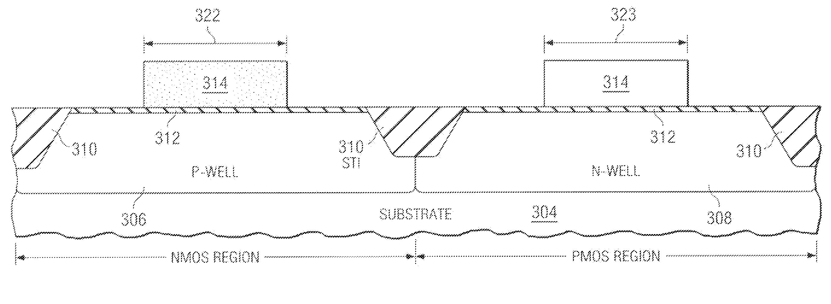
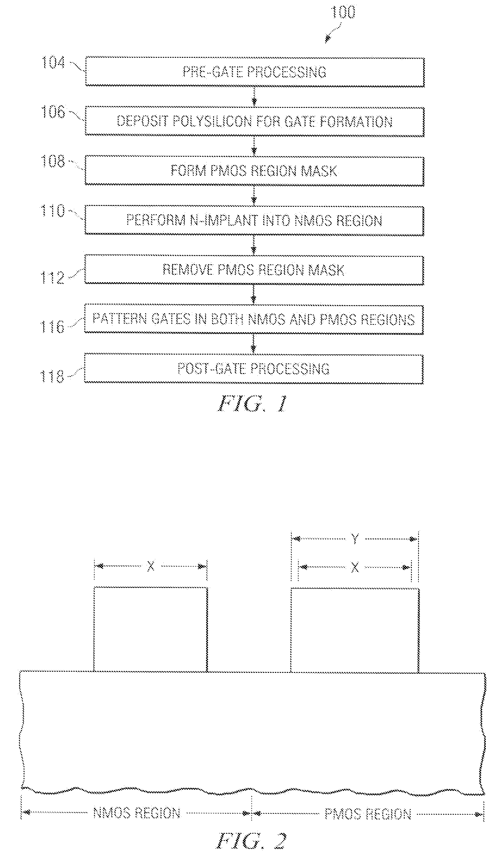
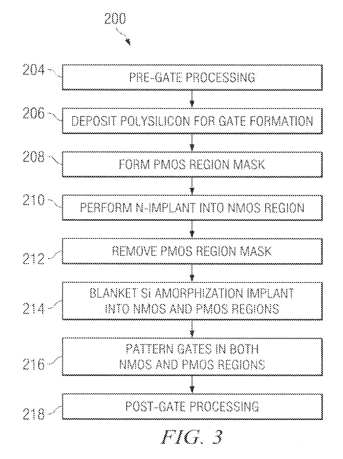
[0020]The invention relates to a method of forming an integrated circuit having NMOS and PMOS transistors. The method reduces the CD gate electrode bias between the NMOS and PMOS transistors by reducing an ...


PUM


Abstract

A method of forming an integrated circuit having an NMOS transistor and a PMOS transistor is disclosed. The method includes performing pre-gate processing in a NMOS region and a PMOS region over and/or in a semiconductor body, and depositing a polysilicon layer over the semiconductor body in both the NMOS and PMOS regions. The method further includes performing a first type implant into the polysilicon layer in one of the NMOS region and PMOS region, and performing an amorphizing implant into the polysilicon layer in both the NMOS and PMOS regions, thereby converting the polysilicon layer into an amorphous silicon layer. The method further includes patterning the amorphous silicon layer to form gate electrodes, wherein a gate electrode resides in both the NMOS and PMOS regions.

Description

RELATED APPLICATION[0001]This application claims priority to Ser. No. 61 / 017,859 filed Dec. 31, 2007, which is entitled “Reducing Gate CD Bias in CMOS Processing”.FIELD OF INVENTION[0002]The present invention relates generally to semiconductor fabrication, and more particularly to a device and method of forming NMOS and PMOS transistor with a reduced gate critical dimension (CD) bias therebetween.BACKGROUND OF THE INVENTION[0003]PMOS and NMOS transistors are common circuit components in many integrated circuits. Such transistors have a source and drain region formed in a semiconductor body, with a channel region residing therebetween. A gate electrode is formed over the channel. Upon proper biasing of the gate electrode and the source / drain regions, the transistors may be selectively controlled. For example, in some instances the transistors are turned completely on or off, wherein the transistors operate as switches. Alternatively, such devices can also be partially activated, wher...

Claims


Application Information

Patent Timeline
Patent Type & Authority Applications(United States)
IPC IPC(8): H01L21/8238H01L27/092
CPCH01L21/82385H01L21/823842
Inventor MEHRAD, FREIDOONCHOI, JINHANJOHNSON, FRANK SCOTT
Owner TEXAS INSTR INC
Why Eureka
Try Eureka