Display device, method for driving the same, and electronic apparatus

a display device and display method technology, applied in lighting devices, instruments, light sources, etc., can solve problems such as and achieve the effect of eliminating the difference in brightness among pixels and suppressing the variation of the sampling period of video signals

Inactive Publication Date: 2008-05-15
SONY CORP
View PDF5 Cites 141 Cited by
  • Summary
  • Abstract
  • Description
  • Claims
  • Application Information

AI Technical Summary

Benefits of technology

[0012]However, variations in operation characteristics, such as threshold voltage and mobility, of transistors and variations in device characteristics of organic EL elements affect emission brightness, and thus those variations need to be corrected in respective pixel circuits. Display devices in which pixel circuits have a threshold voltage correcting function and a mobility correcting function have been developed. The threshold voltage correcting function can correct variations in threshold voltage of the transistors, and the mobility correcting function can correct variations in mobility of the transistors. Particularly, whether correction of mobility can be normally performed has a great influence on image quality in a display device.
[0013]Correction of mobility is performed by negatively feeding back a current flowing to a transistor that drives a light-emitting element to a gate potential of the transistor. The mobility of the transistor corresponds to its current driving ability. A large mobility causes the driving transistor to supply a large drive current. This drive current is fed back to the gate side of the driving transistor only in a predetermined correcting period. A large mobility also causes a large amount of feedback, and the gate potential is compressed accordingly, so that the drive current is suppressed. In this way, variations in mobility of driving transistors can be corrected in individual pixel circuits.
[0015]The present invention has been made in view of the above-described problems of the related arts, and is directed to providing a display device capable of suppressing variations in mobility correcting period and eliminating a difference in brightness among pixels, and a method for driving the display device.
[0018]The mobility correcting period is defined by the first timing when the emission time controlling transistor is turned ON and the second timing when the sampling transistor is turned OFF. According to the related arts, an effect of an enable pulse is applied to a pulse controlling ON and OFF of the sampling transistor and an edge of the control pulse is shaped in order to suppress variations in sampling period a video signal. Accordingly, the second timing when the sampling transistor is turned OFF can be controlled so that variations do not occur in all pixels. However, if the first timing defining the start of the mobility correcting period varies, it may be impossible to make the mobility correcting period constant among the pixels. According to an embodiment of the present invention, an effect of another enable pulse is applied to the pulse controlling ON and OFF of the emission time controlling transistor so as to shape an edge of the control pulse. Accordingly, the first timing defining the start of the mobility correcting period can be fixed in addition to the second timing defining the end of the mobility correcting period, the same mobility correcting period can be obtained in all the pixels, so that a difference in brightness among the pixels can be eliminated.

Problems solved by technology

The difference in brightness among pixels caused by variations in mobility correcting period is a problem to be overcome.

Method used


Image

  • Display device, method for driving the same, and electronic apparatus
  • Display device, method for driving the same, and electronic apparatus
  • Display device, method for driving the same, and electronic apparatus

Examples


Embodiment Construction

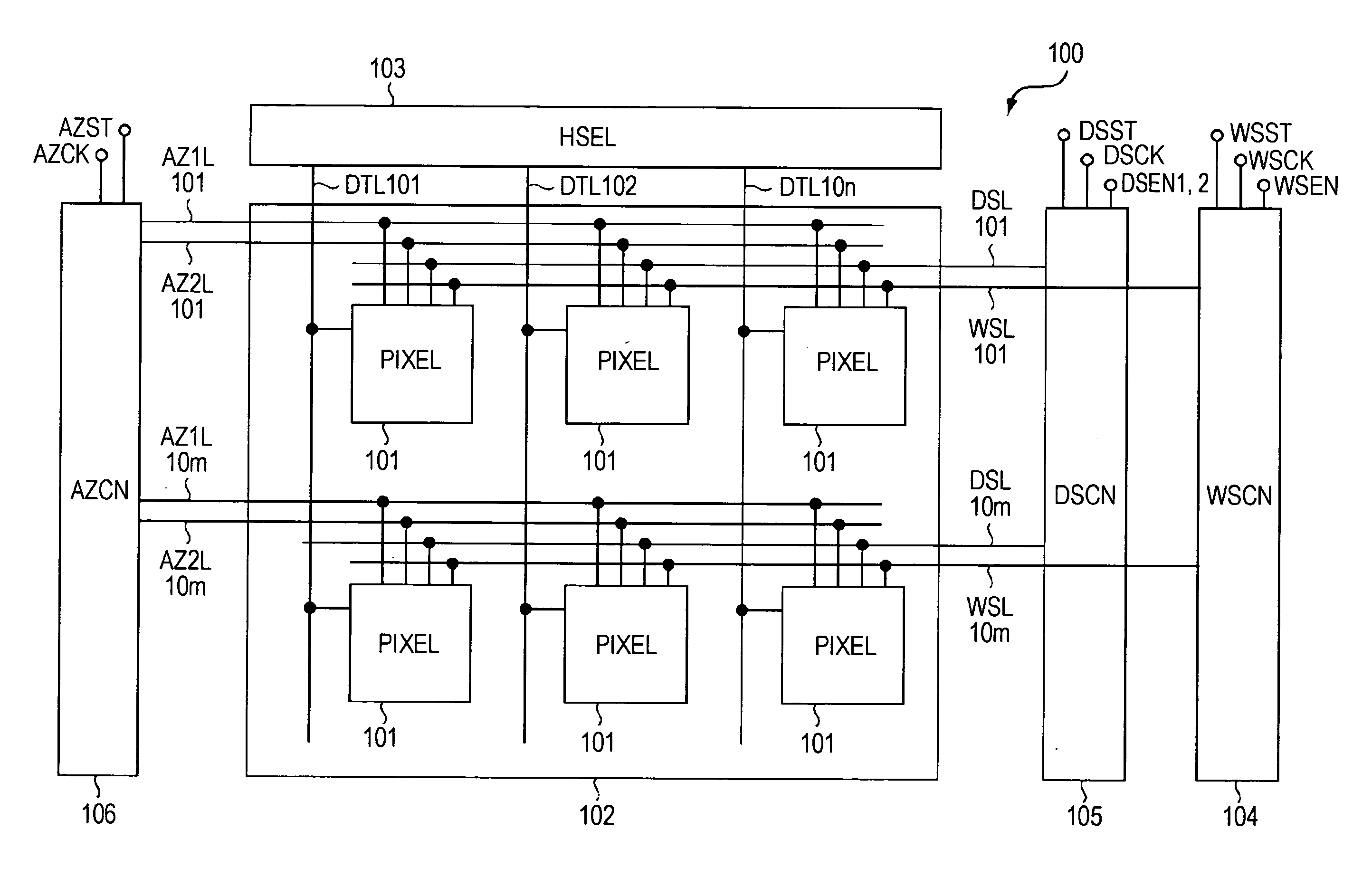
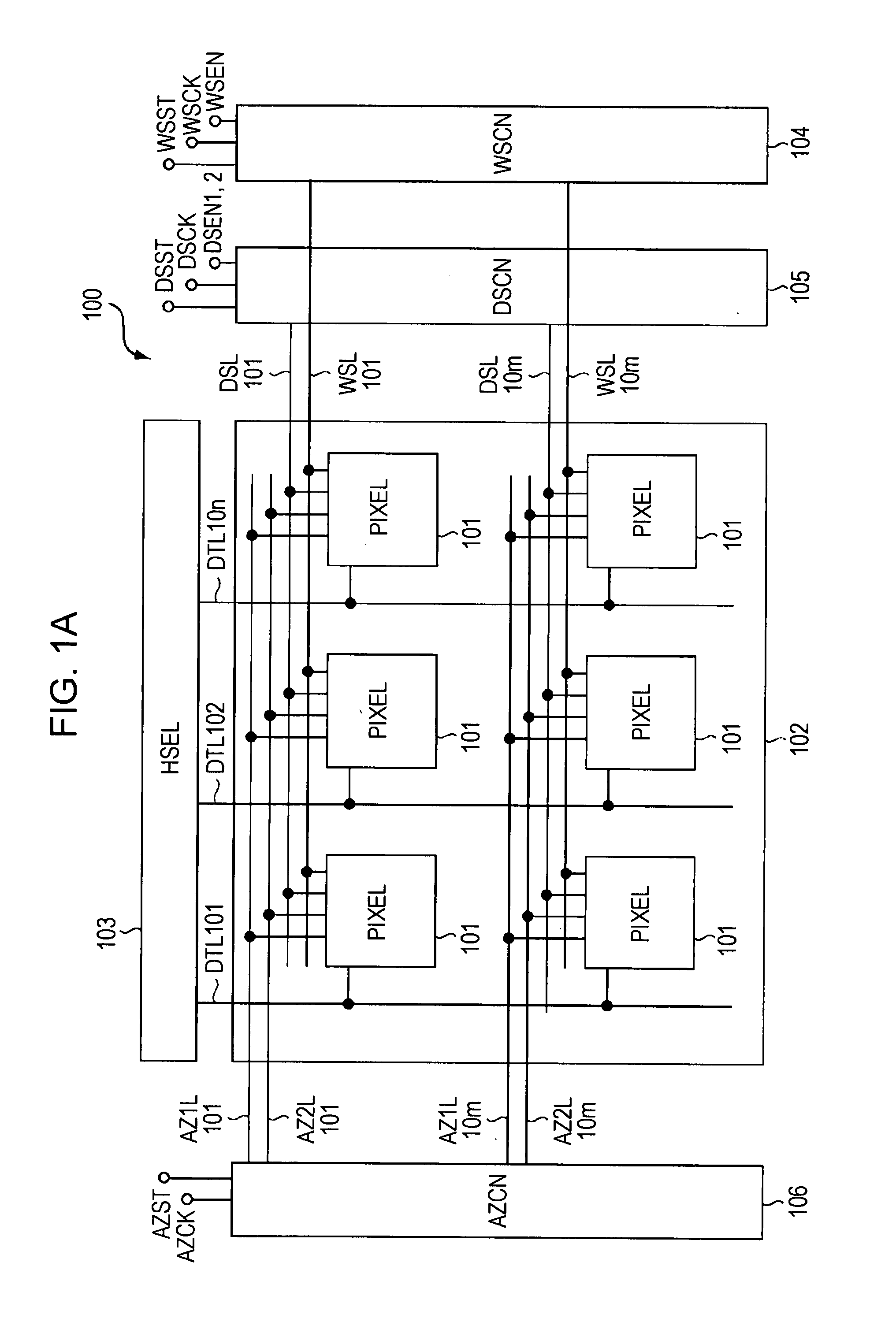
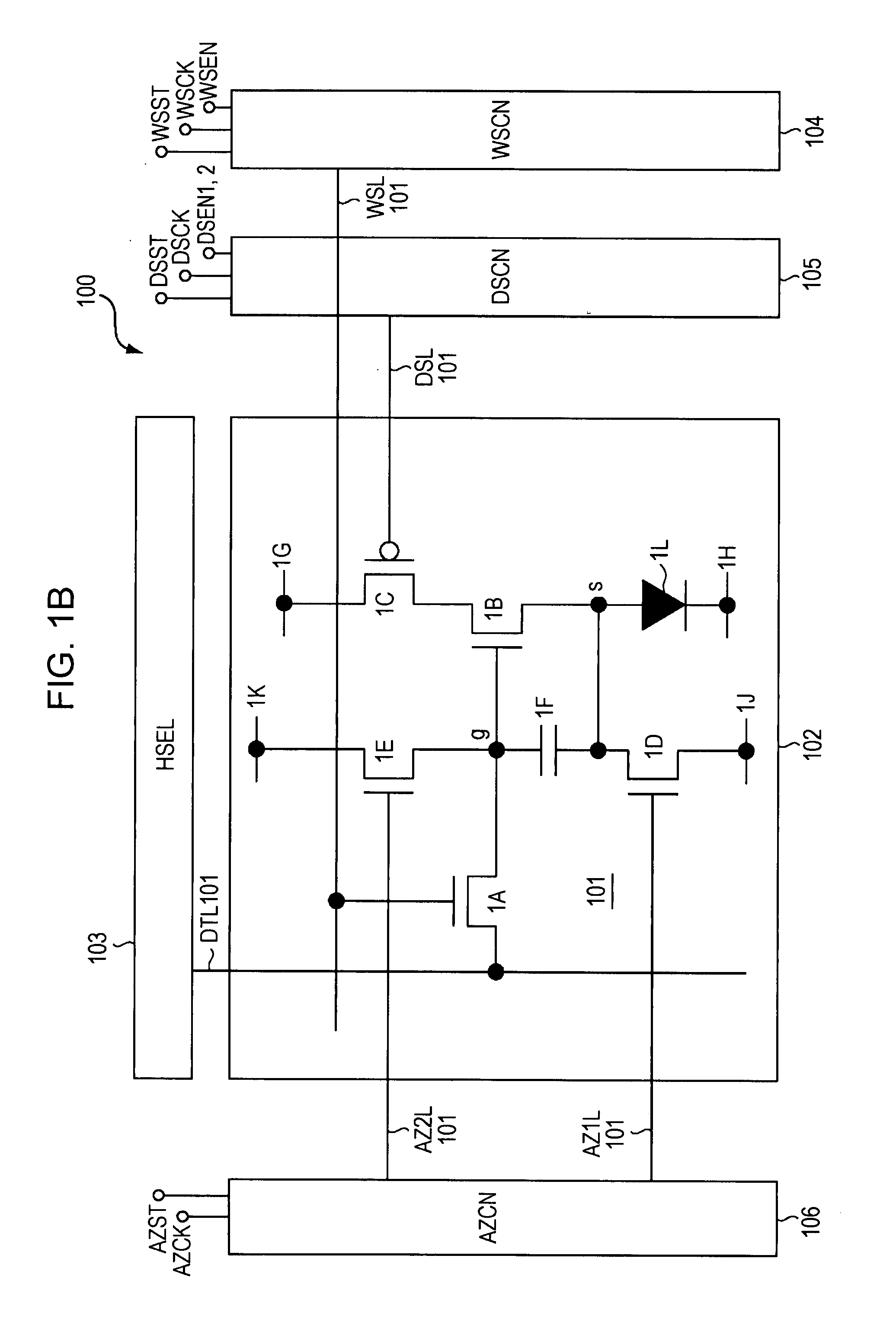
[0044]Hereinafter, embodiments of the present invention are described in detail with reference to the drawings. FIG. 1A is a block diagram showing an entire configuration of a display device 100 according to an embodiment of the present invention. As shown in FIG. 1A, the display device 100 includes a pixel array unit 102 and a peripheral circuit unit. The pixel array unit 102 includes first scanning lines WSL arranged in rows, second scanning lines DSL arranged in rows, signal lines DTL arranged in columns, and pixels 101 arranged in a matrix pattern at intersections of the scanning lines WSL and the signal lines DTL. In the example shown in FIG. 1A, the pixels 101 are arranged in m rows and n columns. When the scanning lines WSL are distinguished from each other, they are referred to as “WSL101” (scanning line in a first row), “WSL10m ” (scanning line in an m-th row), and the like. This is the same for the second scanning lines DSL. Likewise, when the signal lines DTL are distingu...


PUM


Abstract

A display device includes a pixel array unit and a peripheral circuit unit. The pixel array unit includes first scanning lines arranged in rows; second scanning lines arranged in rows; signal lines arranged in columns; and pixels arranged in a matrix pattern at intersections of the scanning lines and the signal lines. The peripheral circuit unit includes a first scanner to supply first control pulses to the first scanning lines; a second scanner to supply second control pulses to the second scanning lines; and a signal driver to supply video signals to the signal lines. Each of the pixels includes at least a sampling transistor; a driving transistor; an emission time controlling transistor; a holding capacitance; and a light-emitting element.

Description

CROSS REFERENCES TO RELATED APPLICATIONS[0001]The present invention contains subject matter related to Japanese Patent Application JP 2006-306127 filed in the Japanese Patent Office on Nov. 13, 2006, the entire contents of which are incorporated herein by reference.BACKGROUND OF THE INVENTION[0002]1. Field of the Invention[0003]The present invention relates to an active matrix display device including light-emitting elements provided for pixels, and to a method for driving the display device. More specifically, the present invention relates to a technique of correcting variations in emission brightness of respective pixels. Also, the present invention relates to electronic apparatuses including the display device.[0004]2. Description of the Related Art[0005]A light-emitting element using a phenomenon of emitting light due to an electric field applied to an organic thin film has been known. Such a light-emitting element is called an organic EL element. Under the present circumstances...

Claims


Application Information

Patent Timeline
Patent Type & Authority Applications(United States)
IPC IPC(8): G09G3/20
CPCG09G3/3233G09G2320/0233G09G2300/0819G09G2300/0814G09G3/20G09G3/30G09G3/32H05B33/12
Inventor UCHINO, KATSUHIDEYAMASHITA, JUNICHITANIKAME, TAKAO
Owner SONY CORP
Why Eureka
Try Eureka