Display device, driving method therefor, and electronic apparatus

a display device and driving method technology, applied in the direction of instruments, computing, electric digital data processing, etc., can solve the problems of large size, difficulty in achieving high-definition display, and self-luminous organic el elements of organic el displays, so as to improve the uniformity of illumination over the screen of the display device

Inactive Publication Date: 2013-10-22
SONY CORP
View PDF9 Cites 1 Cited by
  • Summary
  • Abstract
  • Description
  • Claims
  • Application Information

AI Technical Summary

Benefits of technology

[0008]The drive transistor receives, the input voltage held in the pixel capacitor at the gate thereof, causing the output current to flow between the source and drain thereof, and energizes the light-emitting element. Generally, the intensity of light emitted from the light-emitting element is proportional to the amount of current flowing therethrough. The amount of output current supplied from the drive transistor is controlled by the gate voltage, that is, by the input voltage written to the pixel capacitor. The pixel circuit of the related art controls the amount of current supplied to the light-emitting element by varying the input voltage applied to the gate of the drive transistor according to the input video signal.
[0016]According to an embodiment of the present invention, during the video signal writing period from the time when the sampling transistor is turned on to the time when the sampling transistor is turned off, a scanner included in a peripheral driving unit applies a pulsed control signal to a scanning line to keep the switching transistor on for a limited period of correction time. This adjusts the signal potential stored in the pixel capacitor so as to correct the mobility of the drive transistor. The mobility correction period is defined by the pulse width of the control signal applied to the gate of the switching transistor. It is possible to precisely control the mobility correction period to prevent variations in mobility correction period from pixel to pixel. Thus, luminance uniformity over the screen of the display device can be improved.

Problems solved by technology

However, unlike the liquid crystal pixels of the liquid crystal display, the organic EL elements of the organic EL display are self-luminous.
Although a simple-matrix display is simple in structure, it has problems in its large size and its difficulty achieving high definition display.

Method used


Image

  • Display device, driving method therefor, and electronic apparatus
  • Display device, driving method therefor, and electronic apparatus
  • Display device, driving method therefor, and electronic apparatus

Examples


Embodiment Construction

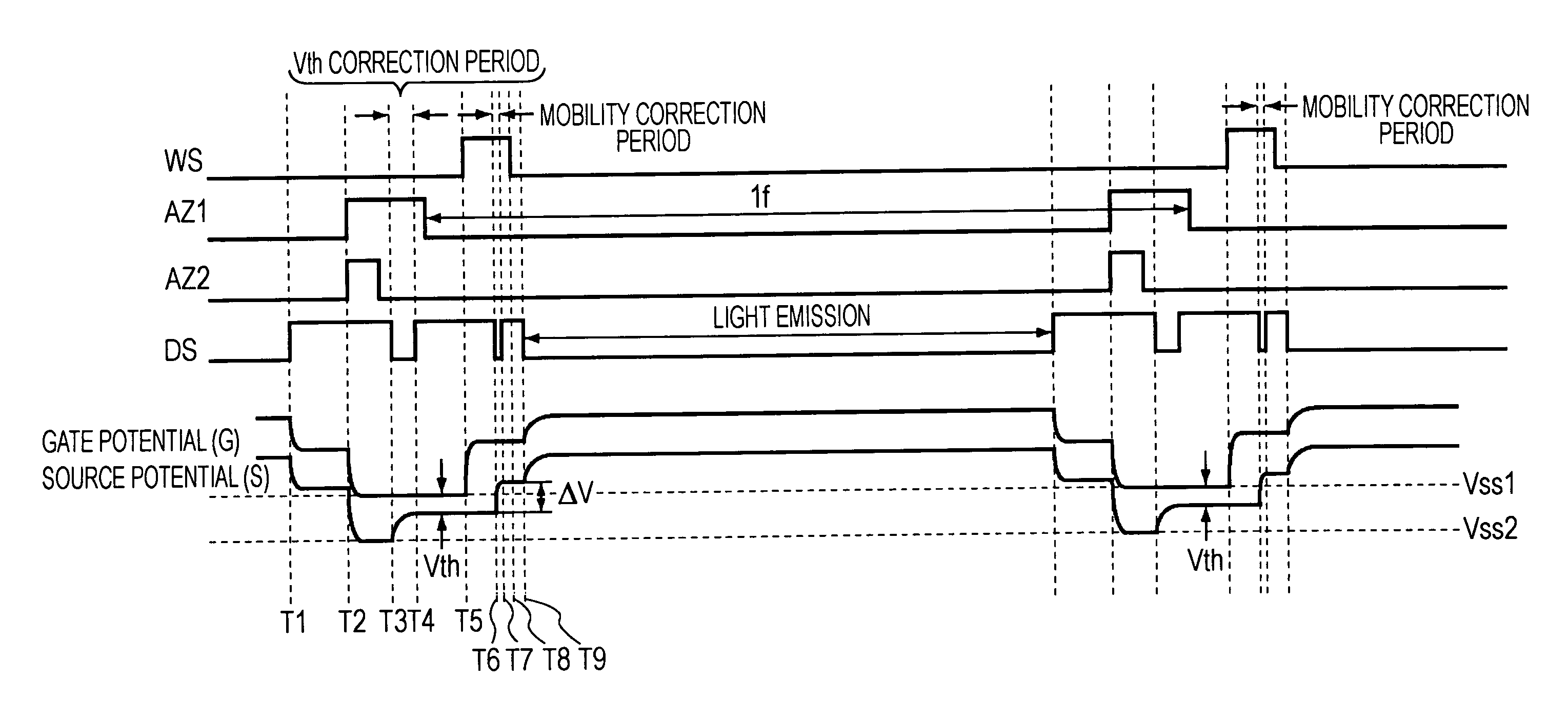
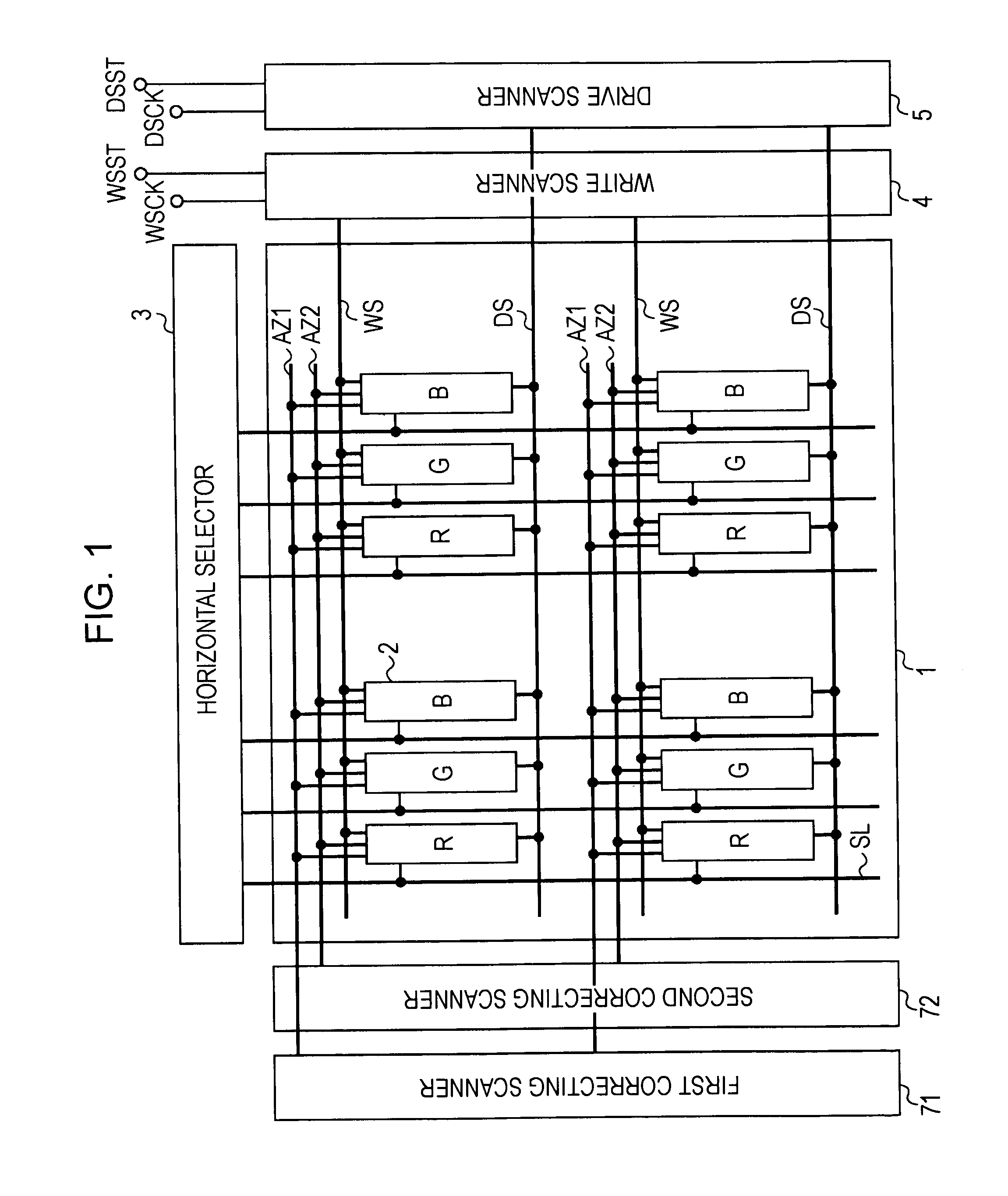
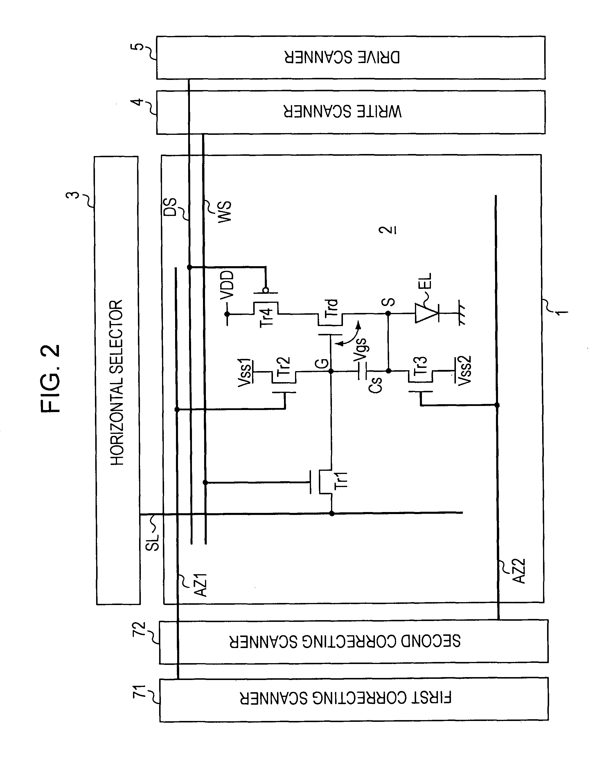
[0035]Hereinafter, embodiments of the present invention will be described in detail with reference to the drawings. FIG. 1 is a schematic block diagram illustrating an overall configuration of a display device according to an embodiment of the present invention. As illustrated, the image display device basically includes a pixel array 1 and a drive unit including a scanner part and a signal part. The pixel array 1 includes scanning lines WS, scanning lines AZ1, scanning lines AZ2 and DS arranged in rows; signal lines SL arranged in columns; a matrix of pixel circuits 2 connected to the scanning lines WS, AZ1, AZ2, DS and to the signal lines SL; and a plurality of power supply lines for supplying a first potential Vss1, a second potential Vss2, and a third potential VDD necessary for operation of each of the pixel circuits 2. The signal part includes a horizontal selector 3, which supplies video signals to the signal lines SL. The scanner part includes a write scanner 4, a drive scan...


PUM


Abstract

A display device includes a pixel array and a drive unit that drives the pixel array. The pixel array includes first and second scanning lines in rows, signal lines in columns, a matrix of pixels arranged at respective intersections of the scanning lines and the signal lines, power supply lines that supply power to each of the pixels, and ground lines. The drive unit includes a first scanner that sequentially supplies first control signals to the corresponding first scanning lines to perform line-sequential scanning on the pixels on a row-by-row basis, a second scanner that sequentially supplies second control signals to the corresponding second scanning lines in synchronization with the line-sequential scanning, and a signal selector that supplies video signals to the signal lines in synchronization with the line-sequential scanning. Each pixel includes a light-emitting element, a sampling transistor, a drive transistor, a switching transistor, and a pixel capacitor.

Description

CROSS REFERENCES TO RELATED APPLICATIONS[0001]The present invention contains subject matter related to Japanese Patent Application JP 2007-078218 filed in the Japanese Patent Office on Mar. 26, 2007, the entire contents of which are incorporated herein by reference.BACKGROUND OF THE INVENTION[0002]1. Field of the Invention[0003]The present invention relates to a display device for displaying an image by current-driving light-emitting elements disposed to its respective pixels, to a driving method for the display device and to an electronic apparatus including the display device. More specifically, the present invention relates to a driving method for an active matrix display device in which the current passing through a light-emitting element, such as an organic electroluminescent (EL) element, is controlled by an insulated-gate field-effect transistor in each pixel circuit.[0004]2. Description of the Related Art[0005]An example of such display device is a liquid crystal display in ...

Claims


Application Information

Patent Timeline
Patent Type & Authority Patents(United States)
IPC IPC(8): G06F3/038G09G5/00
CPCG09G3/3233G09G2300/0819G09G2300/0842G09G2300/0861G09G2310/0251G09G2320/043
Inventor YAMASHITA, JUNICHIUCHINO, KATSUHIDE
Owner SONY CORP
Why Eureka
Try Eureka