Organic light-emitting display device and method of fabricating the same

An electroluminescent device, an organic technology, applied in semiconductor/solid-state device manufacturing, electrical components, electric solid-state devices, etc., can solve problems such as distance difference, uneven brightness, poor brightness, etc.

Active Publication Date: 2013-04-24
LG DISPLAY CO LTD
View PDF6 Cites 60 Cited by
  • Summary
  • Abstract
  • Description
  • Claims
  • Application Information

AI Technical Summary

Problems solved by technology

If the second electrode 42 is formed with a thin thickness, the surface resistance increases, and thus the second electrode 42 receives a voltage through the first auxiliary electrode 31 and the second auxiliary electrode 36 formed outside the panel, thus due to the difference between the edge area of ​​the panel and the center portion The difference in distance (and consequent resistance) between the resulting voltage drop
As a result, there is a difference in brightness between the edge portion and the center portion of the panel
This makes the image produced by the device appear uneven in brightness across the device

Method used


Image

  • Organic light-emitting display device and method of fabricating the same
  • Organic light-emitting display device and method of fabricating the same
  • Organic light-emitting display device and method of fabricating the same

Examples


Embodiment Construction

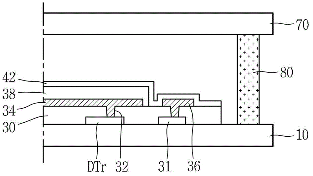
[0026] Figure 4 is a cross-sectional view showing one pixel region including a driving thin film transistor of an organic electroluminescence device according to an embodiment of the present invention. Figure 5 is a sectional view showing an actual pressure drop preventing pattern and banks. Figure 6A to Figure 6E is a plan view showing the shape of the pressure drop prevention pattern according to the embodiment of the present invention.

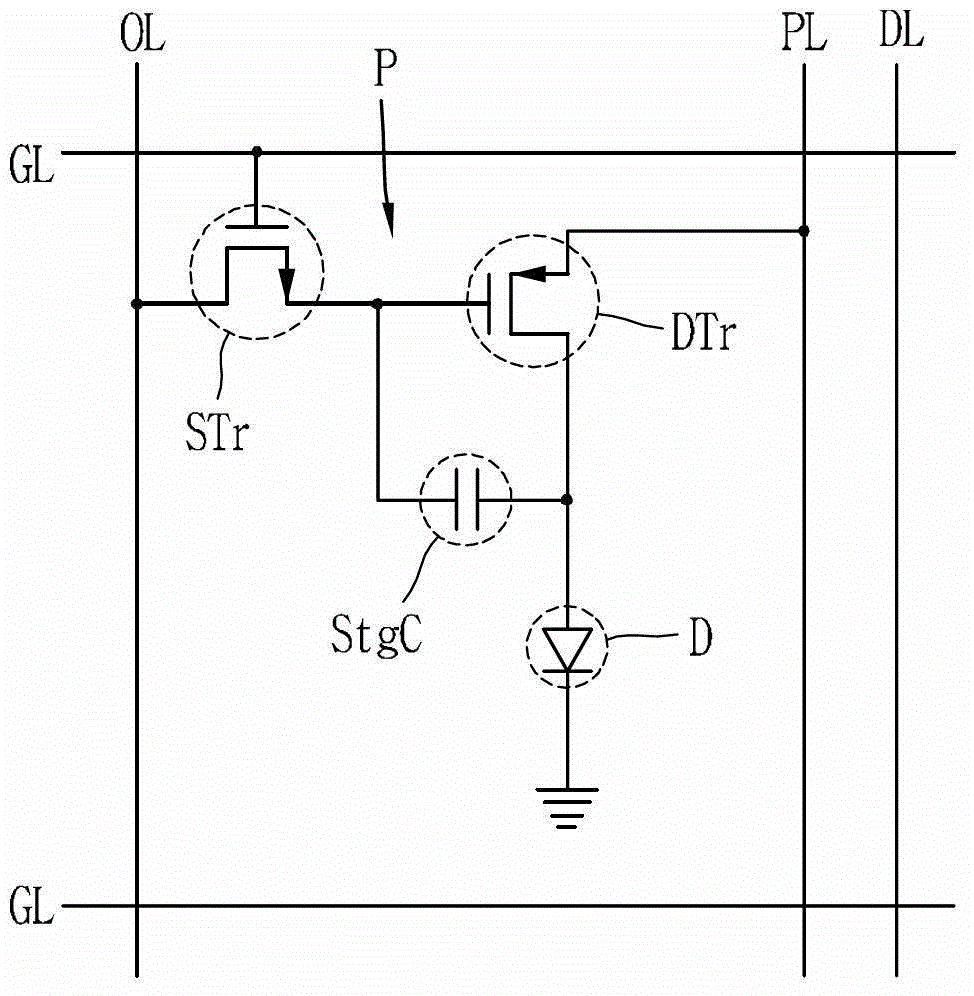
[0027] refer to Figure 4 , the organic electroluminescent device according to an embodiment of the present invention is a top emission type, and the organic electroluminescent device includes a driving and switching transistor (DTr) (as described below, 113, 114 and 115 are combined to form the transistor), The first substrate 110 on which the organic electroluminescent diode (D) and the second substrate 170 for encapsulation are formed.

[0028] A buffer layer 112 is formed on the driving area (DA) of the first substrate 110 . On t...


PUM


Abstract

An organic electro-luminescence device capable of reducing a resistance of a cathode electrode to enhance brightness uniformity at each location within the device is described. The organic electro-luminescence device includes a bank layer formed over a substrate, the bank layer including a first, second, and third portion. A first electrode is formed between the first and second portions of the bank layer. An auxiliary electrode is formed where at least a part of the auxiliary electrode is formed between the second and third portions of the bank layer. A pattern is formed on the auxiliary electrode. An organic material layer formed between the first and second portions of the bank layer. A second electrode formed on the organic material layer, where at least a portion of the second electrode is electrically coupled to the auxiliary electrode.

Description

[0001] Cross References to Related Applications [0002] This application claims priority from Korean Patent Application No. 10-2011-0089277 filed on September 2, 2011, the entire contents of which are incorporated herein by reference. technical field [0003] The invention relates to an organic light-emitting display device and a manufacturing method thereof. Background technique [0004] In recent years, portable electronic devices such as notebooks and personal mobile devices have been increasingly used. These devices include display devices. To maximize their operating time per battery charge, it is desirable to construct these display devices using light-weight and low-power technologies such as flat-panel displays such as liquid crystal displays (LCDs) and organic electroluminescent devices ( FPD). [0005] Organic electroluminescent devices have advantages over other display technologies, such as their high brightness, low operating voltage characteristics, high co...

Claims


Application Information

Patent Timeline
Patent Type & Authority Applications(China)
IPC IPC(8): H01L51/52H01L27/32H01L51/56
CPCH01L27/3246H01L33/62H01L51/5212H10K59/1315H10K59/122H10K50/814H10K50/824H01L21/02107H10K50/805
Inventor 李晙硕金世埈柳俊锡
Owner LG DISPLAY CO LTD
Why Eureka
Try Eureka