Display apparatus, driving method for display apparatus and electronic apparatus

a technology of display apparatus and driving method, which is applied in the direction of instruments, static indicating devices, electroluminescent light sources, etc., can solve the problems of loss of uniformity of screen, difficulty in implementing a large-scale display apparatus having high definition, etc., and achieve the optimization of negative feedback feedback, uniform picture quality, and correction of mobility against dispersion

Inactive Publication Date: 2010-09-21
SONY CORP
View PDF3 Cites 1 Cited by
  • Summary
  • Abstract
  • Description
  • Claims
  • Application Information

AI Technical Summary

Benefits of technology

[0017]In the display apparatus, since the drain-source current of the driving transistor is negatively fed back to the gate input side of the driving transistor, the current value of the drain-source current of the driving transistor is uniformized among the pixels which may be different in mobility. As a result, correction of the mobility against dispersion can be achieved. The feedback amount in the negative feedback can be optimized by adjustment of the correction time of the mobility. The optimum mobility correction time depends upon the signal voltage of the image signal. Here, by using an AC power supply as a power supply to the final stage buffer of the scanning circuit, a scanning signal of an analog waveform can be produced. Then, mobility correction time suitable for the signal voltage of the image signal can be set by determining the mobility correction time using the scanning signal of an analog waveform.
[0018]With the display apparatus, the dependence of the drain-source current of the driving transistor upon the mobility can be canceled in response to the signal voltage of the image signal by setting mobility correction time suitable for the signal voltage of the image signal. Consequently, a display image of uniform picture quality free from stripes, ununiform luminance or the like arising from the difference in mobility of the driving transistor among the different pixels can be obtained.

Problems solved by technology

However, although the display apparatus of the simple matrix type is simple in structure, it has such a problem that it is difficult to implement a display apparatus of a large size having high definition.
Since, if the threshold voltage Vth is different among different driving transistors, then the values of current flowing through the driving transistors exhibit dispersion, even if the same voltage is applied to the gate of the driving transistors, the organic EL elements emit light in different luminance, resulting in loss of the uniformity of the screen.

Method used


Image

  • Display apparatus, driving method for display apparatus and electronic apparatus
  • Display apparatus, driving method for display apparatus and electronic apparatus
  • Display apparatus, driving method for display apparatus and electronic apparatus

Examples


first embodiment

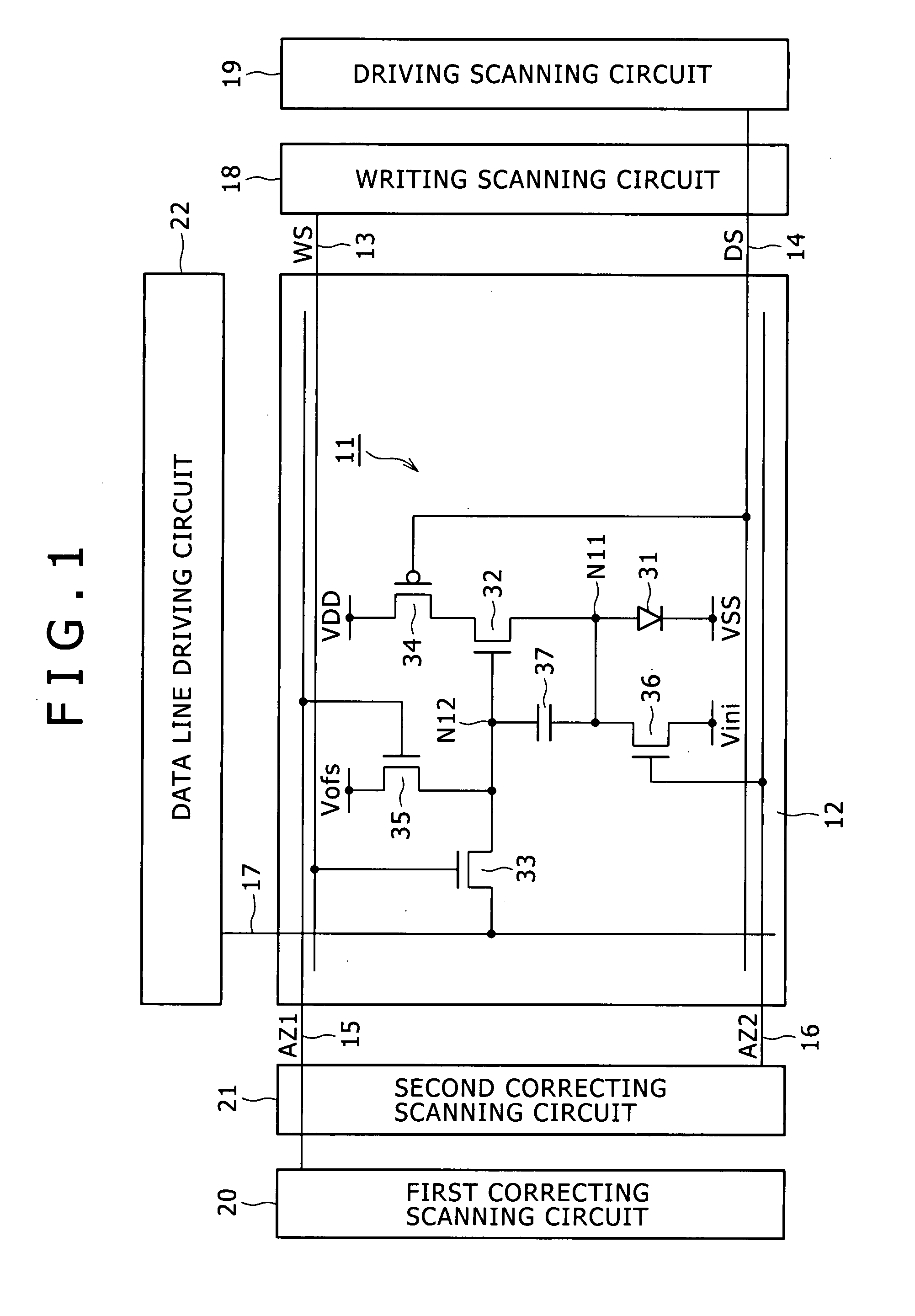
[0139]FIG. 8 shows a circuit configuration of the writing scanning circuit 18A according to a first embodiment of the present invention. In particular, FIG. 8 shows a circuit configuration of a shift stage (i) which corresponds to the ith row of the pixel array section 12. However, also the other shift stages have a same circuit configuration.

[0140]Referring to FIG. 8, the shift stage (i) of the writing scanning circuit 18A according to the first embodiment of the present invention includes a shift register stage 181(i) including a logic circuit, a level conversion circuit 182(i), and an output circuit formed from, for example, two stages of buffers 183(i) and 184(i). It is to be noted, however, that the level conversion circuit 182(i) may not basically required but is provided where it is necessary to perform level conversion of an output signal of the shift register stage 181(i).

[0141]The writing scanning circuit 18A includes a shift register formed from a number of shift register...

first example

[0151]FIG. 11 shows a first example of a circuit configuration of the VDDVbAC production circuit 40. Referring to FIG. 11, the VDDVbAC production circuit 40 includes, an input SW11, for example, two discharge switches SW12 and SW13, two current sources I11 and I12 and a capacitor C.

[0152]The input switch SW11 selectively fetches the power supply potential VDDVb of the DC power supply. The capacitor C is connected between the output terminal of the input switch SW11 and the power supply potential VSS, which is, in the arrangement shown in FIG. 11, the ground potential GND, and is charged by the power supply potential VDDVb inputted through the input switch SW11.

[0153]The discharge switch SW12 and the current source I11 are connected in series and the discharge switch SW13 and the current source I12 are connected in series, both between the output terminal of the input switch SW11, which is the input terminal of the capacitor C, and the power supply potential VSS. The current value of...

second example

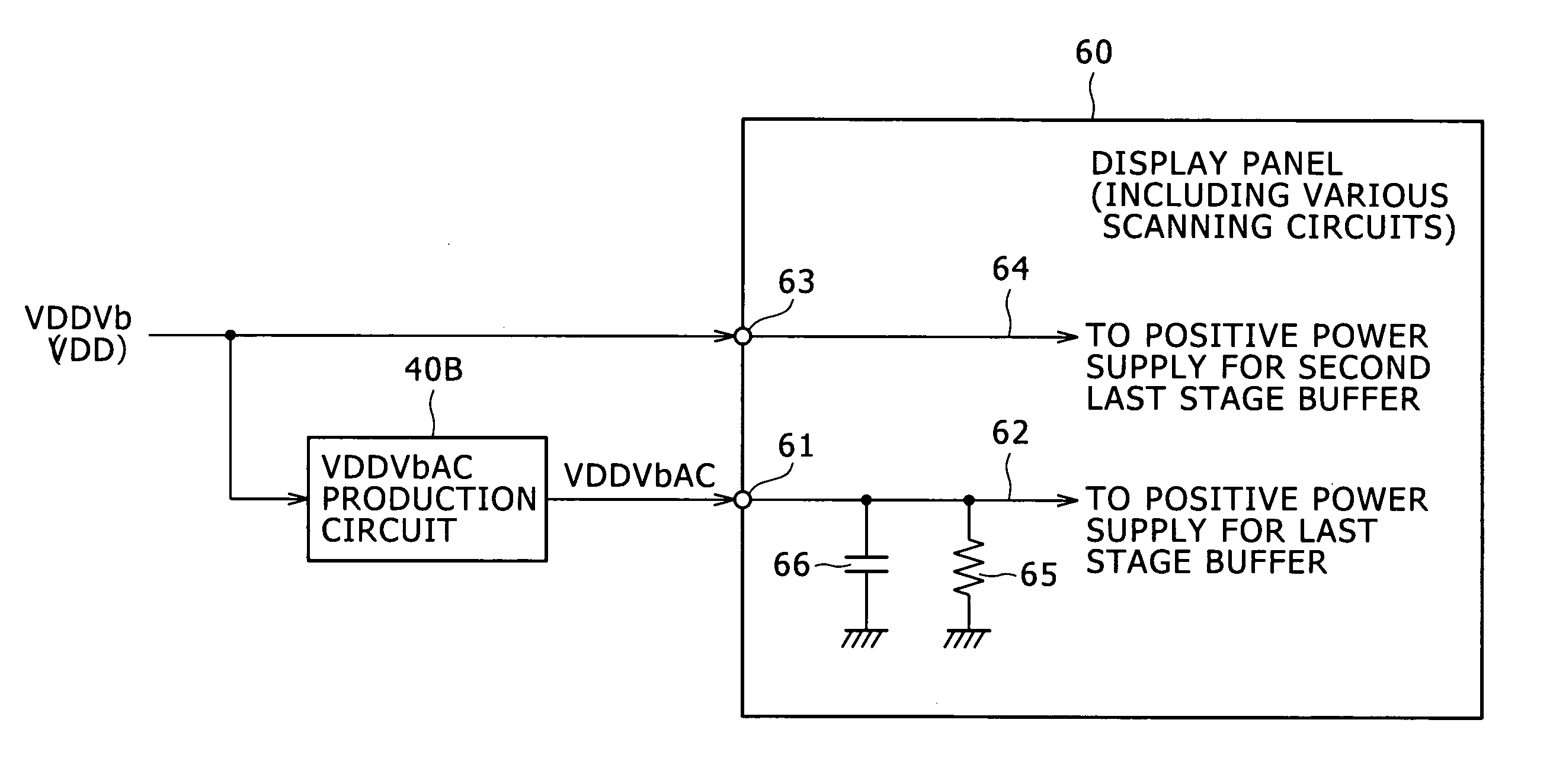
[0163]FIG. 14 shows a second example of a circuit configuration of the VDDVbAC production circuit 40.

[0164]Referring to FIG. 14, the VDDVbAC production circuit 40B according to the second example includes an input switch SW11, for example, two resistance elements R11 and R12 and two discharge switches SW12 and SW13, and a capacitor C.

[0165]In particular, the VDDVbAC production circuit 40B includes the resistance elements R11 and R12 in place of the current sources I11 and I12 of the VDDVbAC production circuit 40A according to the first example. The resistance element R12 has a resistance value set higher than that of the resistance element R11. As a result, a discharge path formed from the resistance element R11 and the switch SW12 passes current of a current value higher than that of another discharge path formed from the resistance element R12 and the switch SW13.

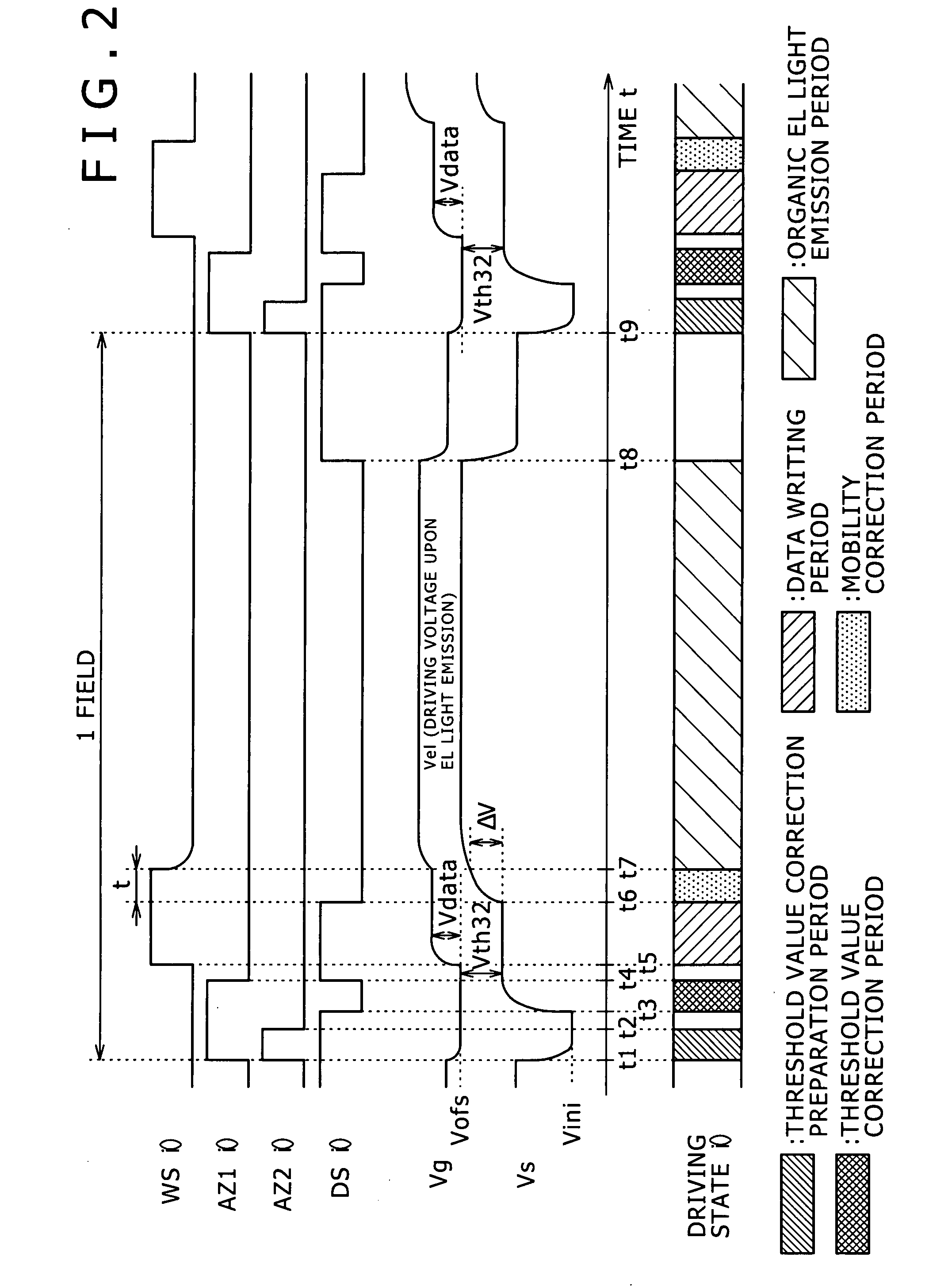
[0166]FIG. 15 illustrates a timing relationship of on / off driving of the input switch SW11 and the discharge switches S...


PUM


Abstract

Disclosed herein is a display apparatus, including: a pixel array section wherein a plurality of pixel circuits each including an electro-optical element, a driving transistor, a sampling transistor and a capacitor are disposed in a matrix; a dependence cancellation section configured to negatively feed back, within a correction period before said electro-optical element emits light in a state wherein the image signal is written by said sampling transistor, drain-source current of said driving transistor to the gate input side of said driving transistor to cancel the dependence of the drain-source current of said driving transistor on the mobility; and a scanning section configured to use an AC power supply as a power supply to a last stage buffer of an output circuit to produce a scanning signal which defines the correction period.

Description

CROSS REFERENCES TO RELATED APPLICATIONS[0001]The present invention contains subject matter related to Japanese Patent Application JP 2006-210619 and JP 2007-139016 filed in the Japan Patent Office on Aug. 2, 2006 and May 25, 2007, respectively, the entire contents of which being incorporated herein by reference.BACKGROUND OF THE INVENTION[0002]1. Field of the Invention[0003]This invention relates to a display apparatus, a driving method for a display apparatus and an electronic apparatus, and more particularly to a display apparatus wherein a plurality of pixel circuits each including an electro-optical element are disposed in a matrix, a driving method for the display apparatus and an electronic apparatus which includes the display apparatus.[0004]2. Description of the Related Art[0005]In recent years, in the field of image display apparatus, an organic EL (electroluminescence) display apparatus has been developed and commercialized wherein a large number of pixel circuits each in...

Claims


Application Information

Patent Timeline
Patent Type & Authority Patents(United States)
IPC IPC(8): G09G3/30
CPCG09G3/3233G09G3/3266G09G2300/0819G09G2300/0842G09G2300/0852G09G2310/0256G09G2310/0289G09G2320/043G09G2330/02G09G3/20G09G3/30G09G3/32H05B33/12
Inventor ASANO, MITSURUFUJIMURA, HIROSHIJINTA, SEIICHIROTOMIDA, MASATSUGU
Owner SONY CORP
Why Eureka
Try Eureka