Method for driving pixel circuit, electro-optic device, and electronic apparatus

a technology of electrooptic devices and circuits, applied in static indicating devices, instruments, electroluminescent light sources, etc., can solve the problems of reducing an aperture ratio and consuming resistor power, so as to reduce power consumption and reduce the aperture ratio , the effect of reducing the mobility of the driver transistor

Active Publication Date: 2012-09-25
138 EAST LCD ADVANCEMENTS LTD
View PDF15 Cites 1 Cited by
  • Summary
  • Abstract
  • Description
  • Claims
  • Application Information

AI Technical Summary

Benefits of technology

[0007]An advantage of some aspects of the invention is that power consumption can be reduced, and at the same time, a variation in mobility of a driver transistor can be corrected without reducing an aperture ratio.
[0009]With this method, in the initialization period, since the first transistor is turned on, the driver transistor is diode-connected. In such a case, because the second transistor is operated in the saturation region thereof, the gate of the driver transistor is biased at a potential obtained in accordance with the mobility of the driver transistor, thereby obtaining a gate potential of the driver transistor. The gate potential of the driver transistor is maintained across a gate capacitance thereof. Accordingly, in the writing period, when a data potential corresponding to a gradation is supplied to the other terminal of the capacitive element, the data potential is superimposed on the potential obtained in accordance with the mobility at the gate of the driver transistor, and the superimposed potential is maintained across the gate capacitance. As a result, the mobility of the driver transistor can be corrected. Furthermore, because no resistor is used, power to be consumed by a resistor can be reduced, and an aperture ratio can be improved.
[0010]It is preferable that the method for driving a pixel circuit include supplying the fixed potential to the other terminal of the capacitive element and supplying a potential allowing the second transistor to be turned off to the gate of the second transistor in a compensation period provided between the initialization period and the writing period. In the first aspect of the invention, a gate-to-source voltage of the driver transistor can be approached to the threshold voltage thereof in the compensation period. More specifically, in a case where the mobility and the threshold voltage of the second transistor vary, when the initialization period is finished, a gate potential influenced by the characteristic variation of the second transistor is maintained at the gate of the driver transistor. In the compensation period, the gate potential of the driver transistor is changed so as to reach the threshold voltage thereof. Accordingly, even when the characteristic of the second transistor varies, the negative effect caused by the variation can be reduced. Thus, since the compensation period is provided, the mobility and the threshold voltage can be corrected. Furthermore, a luminance variation due to the characteristic variation of the second transistor can be suppressed. Any constant potential may be used as the fixed potential. However, when the fixed potential is set to the initialization potential, the number of power supplies can be decreased. Additionally, the compensation period is preferably finished before the gate potential of the driver transistor, i.e., the gate-to-source voltage, reaches the threshold voltage.
[0012]In the second aspect of the invention, in the initialization period, since the potential of the first control signal is set to the potential allowing the first transistor to be turned on, the driver transistor is diode-connected. In this case, since the potential of the second control signal is set to the predetermined potential allowing the second transistor to be operated in the saturation region thereof, the gate of the driver transistor is biased at a potential obtained in accordance with the mobility thereof, thereby obtaining a gate potential of the driver transistor. The gate potential of the driver transistor is maintained across a gate capacitance thereof. Accordingly, in the writing period, when the fourth transistor is turned on to supply a data potential corresponding to a gradation to the other terminal of the capacitive element, the data potential is superimposed on the potential obtained in accordance with the mobility at the gate of the driver transistor, and the superimposed potential is maintained across the gate capacitance. As a result, the mobility of the driver transistor can be corrected. Furthermore, because no resistor is used, power to be consumed by a resistor can be reduced, and an aperture ratio can be improved.
[0014]In the third aspect of the invention, in the compensation period, the potential of the second control signal is set to the potential allowing the second transistor to be turned off. Accordingly, in the initialization period, the driver transistor is diode-connected, and the gate of the driver transistor is biased at the initialization potential, thereby obtaining a gate potential of the driver transistor. However, in the compensation period, the gate potential of the driver transistor is changed to a potential obtained by subtracting the threshold voltage of the driver transistor from a potential of the source of the driver transistor. This enables the gate potential of the driver transistor to be changed in accordance with the threshold thereof. As a result, not only the mobility but also the threshold can be corrected. Additionally, since the gate potential of the driver transistor is changed so as to reach the threshold voltage in the compensation period, even when the characteristic of the second transistor varies, the negative effect caused by the variation can be reduced. Furthermore, the compensation period is preferably finished before the gate potential of the driver transistor, i.e., the gate-to-source voltage, reaches the threshold voltage.

Problems solved by technology

However, because in the technology of the configuration disclosed in JP-A-2006-251632 (Paragraph 0028), a resistor is provided in a path running from a power supply to a driver transistor, there is a problem that this resistor consumes power.
Additionally, the increase of a dimension occupied by the resistor results in reduction of a dimension of a light-emitting element in a pixel circuit, thereby causing a problem of reducing an aperture ratio.

Method used


Image

  • Method for driving pixel circuit, electro-optic device, and electronic apparatus
  • Method for driving pixel circuit, electro-optic device, and electronic apparatus
  • Method for driving pixel circuit, electro-optic device, and electronic apparatus

Examples


first embodiment

A: Configuration of Electro-Optic Device

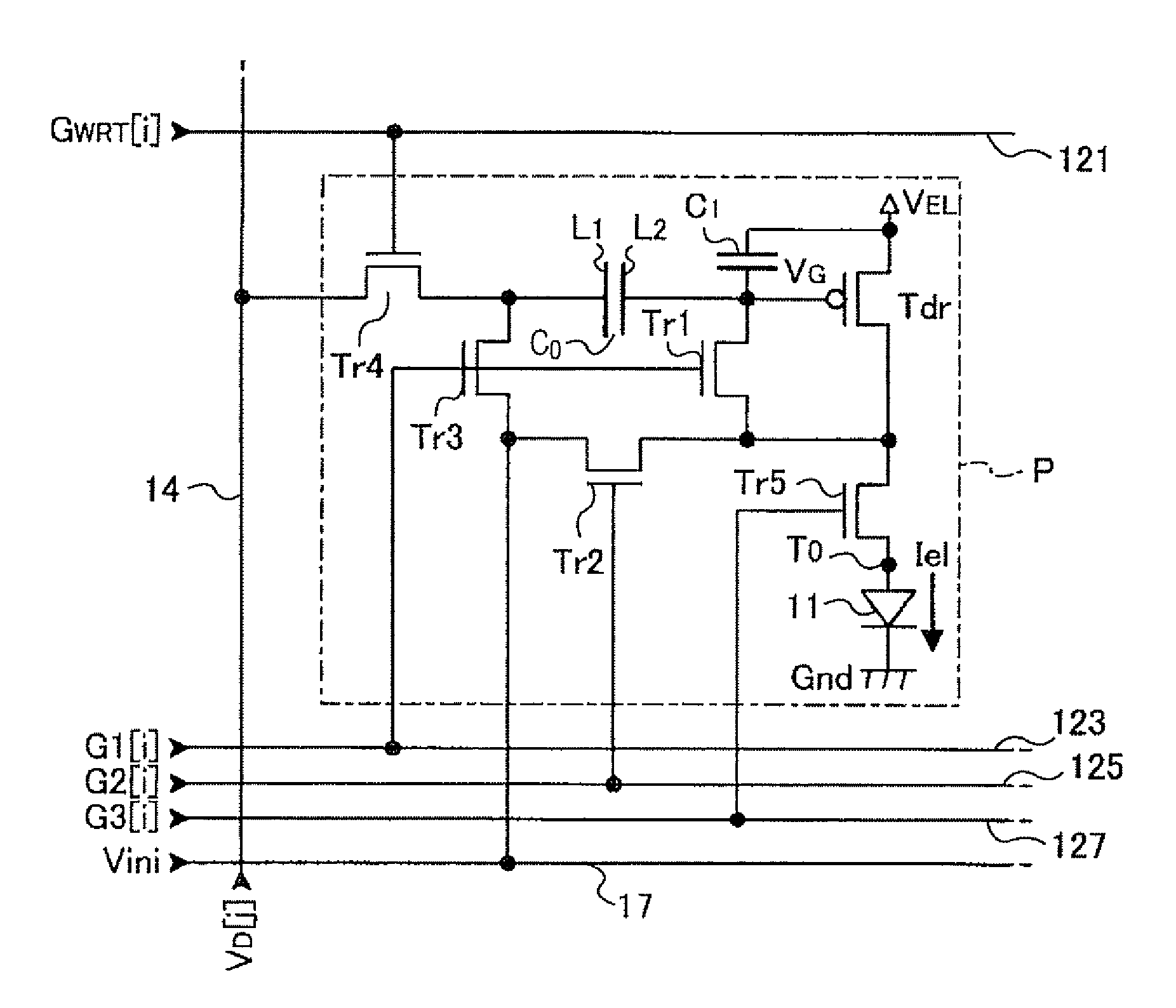
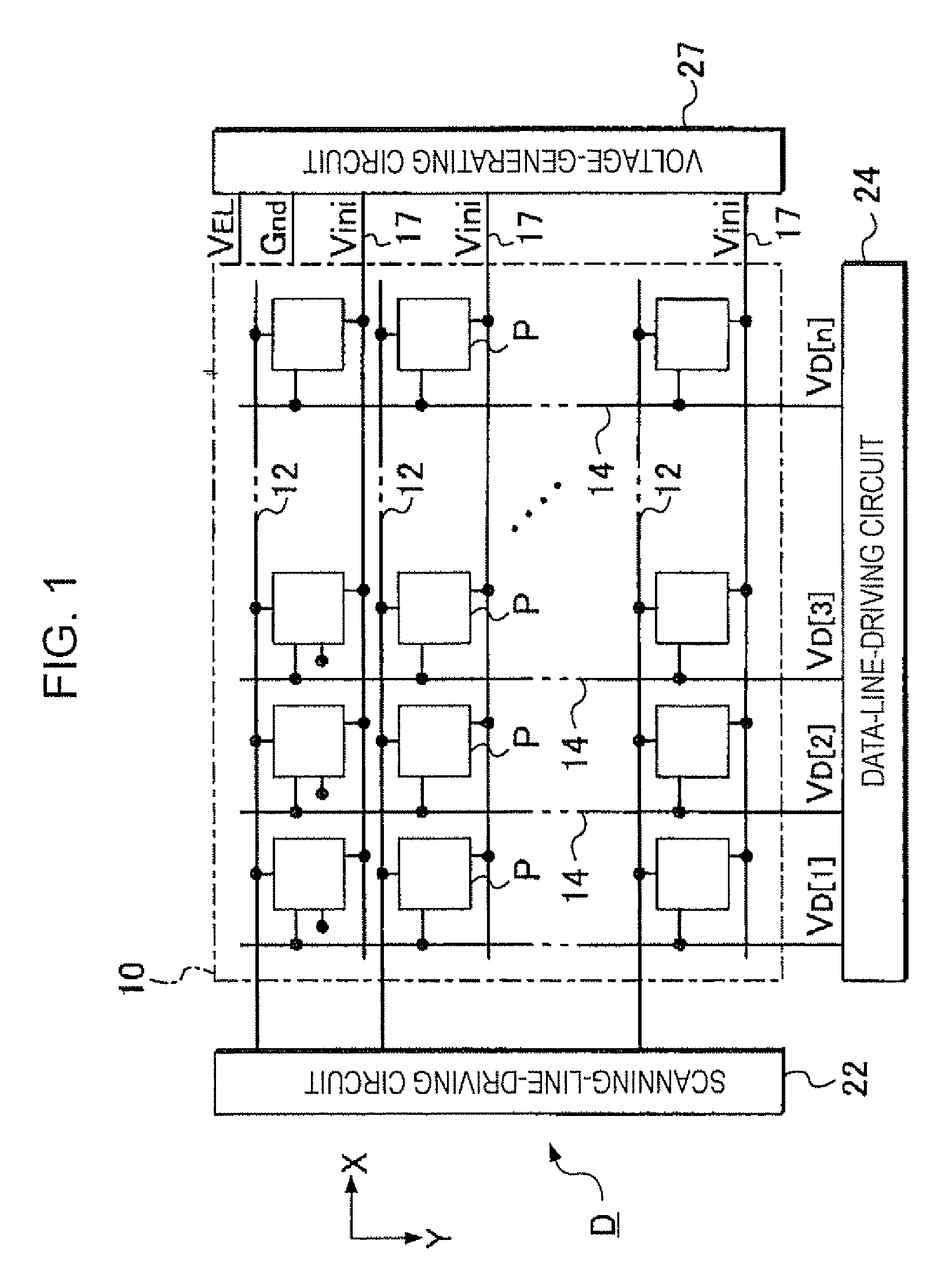
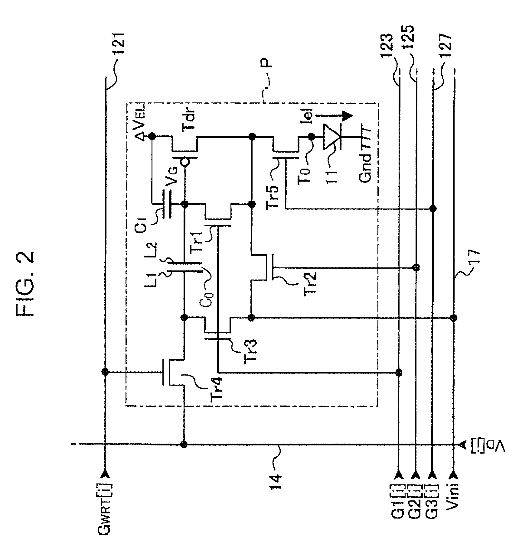
[0032]FIG. 1 is a block diagram of the configuration of an electro-optic device according to a first embodiment of the invention. An electro-optic device D is one of devices employed in various types of electronic apparatuses as units that display images. The electro-optic device D includes a pixel array unit 10 in which pixel circuits P are disposed in the form of a plane, a scanning-line-driving circuit 22 and a data-line-driving circuit 24 that drive the pixel circuits P, and a voltage-generating circuit 27 that generates voltages used in the electro-optic device D. Referring to FIG. 1, the scanning-line-driving circuit 22, the data-line-driving circuit 24, and the voltage-generating circuit 27 are shown as discrete circuits, but a configuration in which a portion of these circuits or all of these circuits are configured into a single circuit may be employed. Additionally, one scanning-line-driving circuit 22 (or one data-line-driving circu...

second embodiment

[0059]An electro-optic device according to a second embodiment has a configuration similar to that of the electro-optic device according to the first embodiment shown in FIG. 1. However, the timing of the first control signal G1[i] in the electro-optic device according to the second embodiment, which is output from the scanning-line-driving circuit 22, is different from that in the electro-optic device according to the first embodiment.

[0060]FIG. 8 is a timing chart of the electro-optic device according to the second embodiment. In this embodiment, a compensation period PH is provided between the initialization period PINT and the writing period PWRT. In the compensation period PH, the characteristic variation of the second transistor Tr2 is corrected.

[0061]As in the case of the first embodiment, suppose that there are provided two driver transistors Tdr, namely, a driver transistor Tdr having Characteristic A and a driver transistor Tdr having Characteristic B, the threshold Vth of...


PUM


Abstract

There is provided a method for driving a pixel circuit including a light-emitting element that emits light whose amount corresponds to a driving current, a driver transistor that supplies the driving current to the light-emitting element, a first transistor provided between a gate of the driver transistor and a drain of the driver transistor, a second transistor provided between the drain of the driver transistor and a node used to supply an initialization potential, and a capacitive element one terminal of which is connected to the gate of the driver transistor. In an initialization period in which the first transistor is turned on, the method for driving a pixel circuit includes supplying a fixed potential to the other terminal of the capacitive element and supplying a predetermined potential allowing the second transistor to be operated in a saturation region thereof to a gate of the second transistor. In a writing period after the initialization period is finished, the method for driving a pixel circuit includes supplying a potential corresponding to a gradation to be displayed to the other terminal of the capacitive element.

Description

BACKGROUND[0001]1. Technical Field[0002]The present invention relates to a technology for controlling the behaviors of various types of electro-optic elements, such as light-emitting elements formed of an organic electroluminescent (EL) material.[0003]2. Related Art[0004]Regarding an electro-optic element of one of these types, a gradation (typically, a luminance) thereof is changed by supplying a current thereto. A configuration in which this current (hereinafter, referred to as a “driving current”) is controlled by a transistor (hereinafter, referred to as a “driver transistor”) has been suggested in the related art.[0005]Since there is a problem that a variation in gradation among electro-optic elements occurs due to a variation in mobility among driver transistors, in order to solve the problem, for example, JP-A-2006-251632 (Paragraph 0028) discloses a configuration in which a resistor is provided between a driver transistor and a power supply to realize a self-correction of a ...

Claims


Application Information

Patent Timeline
Patent Type & Authority Patents(United States)
IPC IPC(8): G09G5/00
CPCG09G3/3233G09G2300/0465G09G2320/043G09G2300/0852G09G2300/0861G09G2300/0819G09G3/20G09G3/30G09G3/32H05B33/12
Inventor TAKAHASHI, KASORI
Owner 138 EAST LCD ADVANCEMENTS LTD
Why Eureka
Try Eureka