Method for improving a printed circuit board development cycle

a technology of printed circuit boards and development cycles, applied in the direction of instrumentation, program control, inspection/indentification of circuits, etc., can solve the problems of difficult automation of points, adversely affecting surrounding circuitry, and changing the transmission line characteristics of traces over which high-speed signals are communicated, so as to improve the time-to-market of pcb assemblies

Inactive Publication Date: 2008-06-19
JACOBSEN CHRIS R +2
View PDF12 Cites 9 Cited by
  • Summary
  • Abstract
  • Description
  • Claims
  • Application Information

AI Technical Summary

Benefits of technology

[0012]The present invention is a technique for improving the time-to-market of a PCB assembly through automation of PCB test pad insertion and fixture probe insertion. During the PCB design stage, the invention utilizes bead probe technology and a test pad location algorithm to automatically position and insert test pads in a PCB design. During the fixture design stage, the invention utilizes a fixture probe location algorithm to automatically position and insert fixture probes in a corresponding test fixture design. The test pad location algorithm and fixture probe location algorithm each utilizes a common probe location algorithm that ensures that fixture probe locations correspond to test pad locations on the PCB under test.

Problems solved by technology

However, several steps in the PCB development cycle are still performed mainly by manual intervention and iterative effort.
For example, as illustrated in FIG. 1, the addition of test pads to the circuit during the PCB design stage and the manual addition of board pushers for push-down top gate fixtures during the fixture development stage have to this point been difficult to automate.
Furthermore, the size of a test pad is also determined by pointing errors in probe placement that may cause lateral offsets.
Because conventional test pads occupy area on the trace layer, the addition of test pads to the PCB design often require rerouting of nets of the PCB design.
The addition of test pads to the design using conventional techniques also carries risks in adversely affecting surrounding circuitry or changing the transmission line characteristics of the traces over which high-speed signals are communicated.
Because the test pad insertion step requires mainly manual effort and is iterative in nature, this step, as illustrated in FIG. 1, might add several days (e.g., 5 days in the example shown) to the PCB design process, yet still not result in 100% probing access.
The addition of test pads to the design has not yet been fully or even substantially automated.
Using conventional test pad fabrication technologies, however, implementation of alternate plural probing locations along the nets are rare since adding even a single test pad to a net, as described above, is so painful in terms of board real estate, risk of adverse impact to circuit performance, time, and cost.
If the counteracting forces of the probes and board pushers are not evenly distributed across the entire board, the PCB will flex and may cause faulty or even fatal test results.
However, even with a top push-down gate 250, if the counteracting forces of the probes and board pushers are not evenly distributed across the entire board, the PCB will flex and may cause stresses that can damage solder connections or even the components themselves.
However, there is no existing automated technique for determining locations of board pushers in a fixture.
Board pusher layout can be time-consuming, and since done manually, may not truly minimize board flex.

Method used


Image

  • Method for improving a printed circuit board development cycle
  • Method for improving a printed circuit board development cycle
  • Method for improving a printed circuit board development cycle

Examples


Embodiment Construction

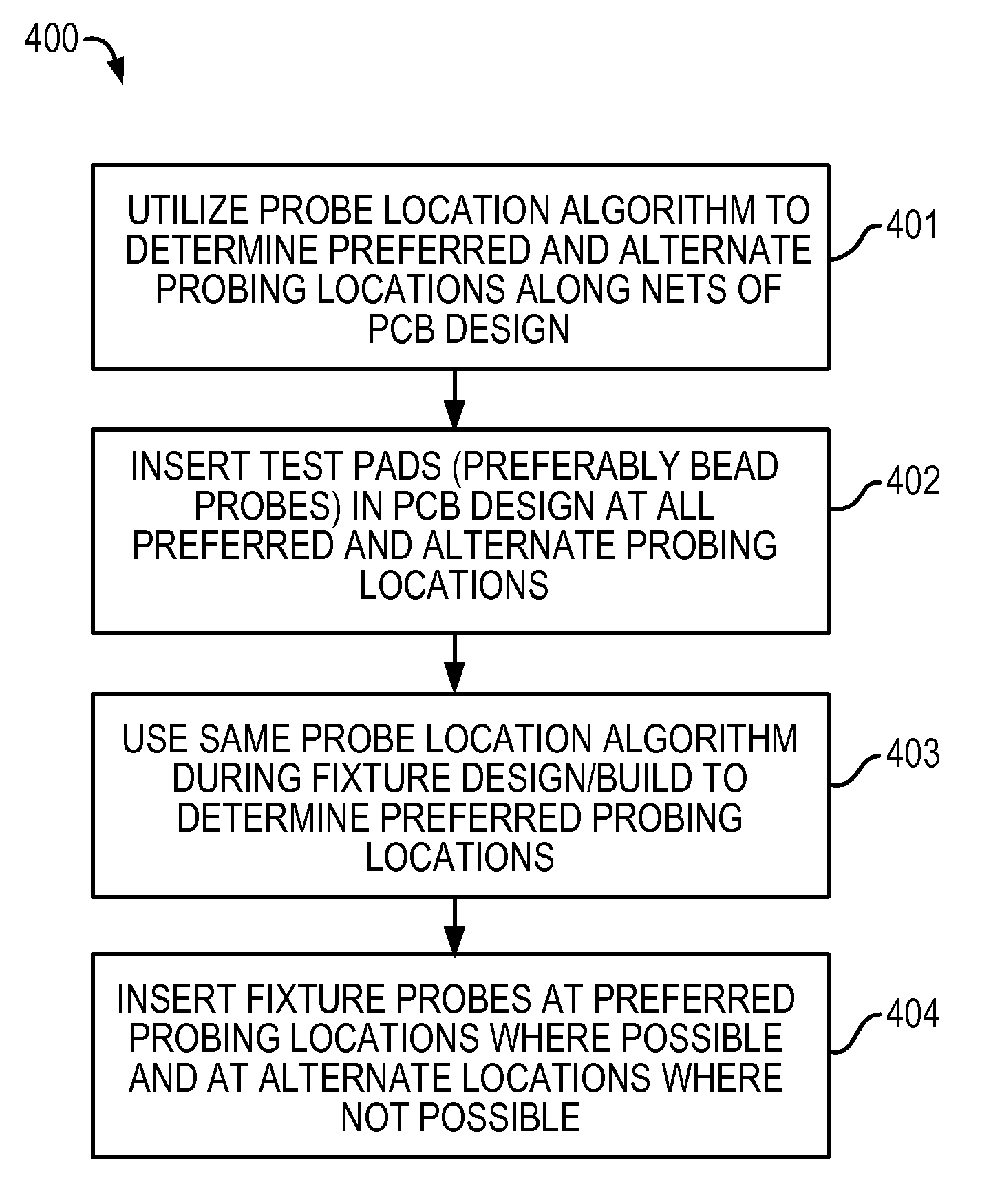
[0023]For purposes of clarity, the following terms are defined:

[0024]“net”—a signal transmission line which passes signals between two or more endpoints over an electrically conductive path; may be implemented as one or more of any of, including combinations of, the following: a trace, a via, a wire, a component lead, a solder ball, a wire bond, or any other electrically conductive element electrically connected between the two or more endpoints and through which the signal passes;

[0025]“test pad”—a point on a net accessible for probing, typically characterized by a surface area large enough to accommodate a probe head;

[0026]“fixture probe”—an electrically conductive element of a tester fixture which operates as a passive transmission line at least between a first end and a second end of the electrically conductive element, the first end configured to electrically contact a test pad of a circuit and the second end configured to electrically contact another electrical component of in...


PUM


Abstract

Techniques for automating test pad insertion in a printed circuit board (PCB) design and fixture probes insertion in a PCB tester fixture are presented. A probe location algorithm predictably determines respective preferred probing locations from among respective sets of potential probing locations associated with a number of respective nets in a PCB design. Test pads, preferably in the form of bead probes, are added to the PCB design at the respective preferred probing locations along with, where feasible, one or more alternate probing locations chosen from among remaining ones of the respective sets of potential probing locations. During fixture design, nets with multiple test pads implemented in the PCB design are processed by the same probe location algorithm used during PCB design to determine the associated preferred probing location and any associated alternate probing locations for said respective nets. Fixture probes are preferably inserted in the PCB tester fixture design at respective preferred probing locations to exactly align with corresponding preferred test pads of a PCB implemented in accordance with the PCB design should the PCB be mounted in a printed circuit board tester fixture implemented in accordance with the PCB tester fixture design.

Description

CROSS-REFERENCE TO RELATED APPLICATION[0001]This application is a divisional of copending application Ser. No. 11 / 009,117 filed on Dec. 10, 2004, the entire disclosure of which is incorporated into this application by reference.BACKGROUND OF THE INVENTION[0002]The present invention relates generally to printed circuit board design and testing, and more particularly to techniques for the printed circuit board development cycle through the use of bead probe technologies and through automation of test pad location during PCB design and fixture probe location during fixture design.[0003]Electronic products typically contain at least one printed circuit board (PCB). A PCB generally includes a plurality of electronic components that are electrically connected together by electrical paths called “nets” that are formed of various combinations of conductive traces, vias, wires, and solder, to form an operational circuit that performs a given function. A conventional PCB development cycle is ...

Claims


Application Information

Patent Timeline
Patent Type & Authority Applications(United States)
IPC IPC(8): G06F17/50
CPCH05K1/0268H05K2203/162H05K3/0005
Inventor JACOBSEN, CHRIS R.PARKER, KENNETH P.HERCZEG, JOHN E.
Owner JACOBSEN CHRIS R
Why Eureka
Try Eureka