Compliant substrate holding assembly

a technology for holding assemblies and semiconductor substrates, applied in positioning apparatuses, metal-working machine components, manufacturing tools, etc., can solve problems such as damage, contamination, scratching, and/or scratching of integrated circuits, and achieve the effects of avoiding collision between substrates, avoiding damage, and avoiding damag

Inactive Publication Date: 2008-07-03
APPLIED MATERIALS INC
View PDF75 Cites 7 Cited by
  • Summary
  • Abstract
  • Description
  • Claims
  • Application Information

AI Technical Summary

Problems solved by technology

Integrated circuits have evolved into complex devices that can include millions of components (e.g., transistors, capacitors and resistors) on a substrate (e.g., semiconductor wafer).
The leaning substrates may contact neighboring substrates positioned in the base plate 102, thus resulting in damage, contamination, and / or scratching.
Additionally, leaning substrates may interfere with substrate transfer or result in collision between substrates during robot transfer.

Method used


Image

  • Compliant substrate holding assembly
  • Compliant substrate holding assembly
  • Compliant substrate holding assembly

Examples


Embodiment Construction

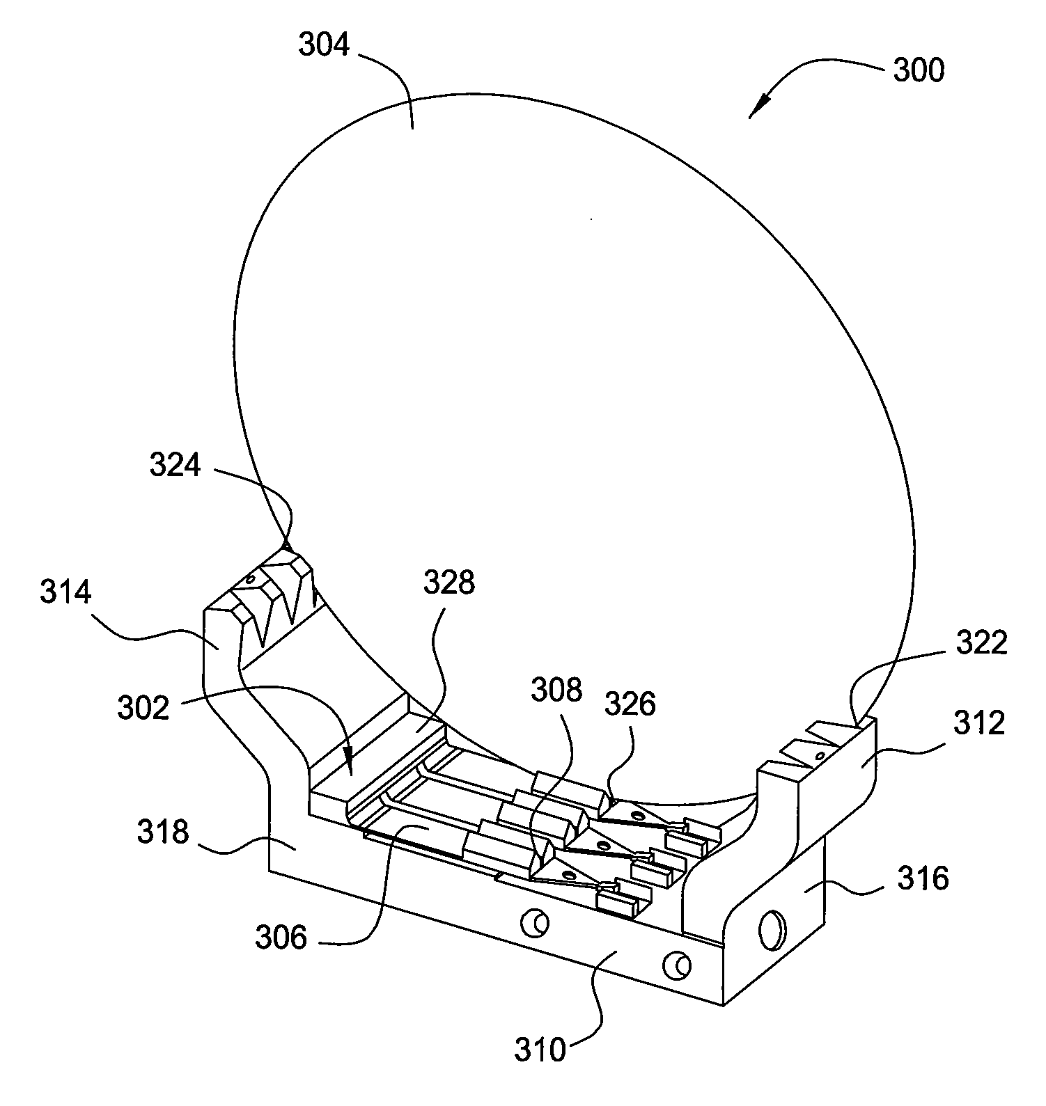
[0022]The present invention provides a method and an apparatus for holding a substrate in a vertical orientation. In one embodiment, the substrate holding assembly has a substrate supporting structure that moves to accommodate substrates of various dimensions and materials, thereby substantially preventing substrate improper positioning, misalignment, and substrate lean. The substrate holding assembly provides three substrate contact points. In another embodiment, a sensor may be provided to accurately detect the presence of a substrate in the holding assembly. The presence of the substrate may be triggered by a change in position of a structure that supports the substrate. Since the change in position of the substrate supporting structure is indicative of the presence of the substrate in the substrate holding assembly, opaque or transparent substrates may be reliably detected.

[0023]FIG. 3 depicts a perspective view of a substrate holding assembly 300 according to one embodiment of ...


PUM


Abstract

Methods and apparatus for holding substrate in a compliant substrate holding assembly are provided. In one embodiment, an apparatus for a compliant substrate holding assembly includes a base plate, a finger disposed on the base plate having a V-shaped slot formed thereon, and two arms disposed on opposite ends of the base plate and each arm having V-shaped slot formed therein. In another embodiment, a method for holding a substrate on a compliant substrate holding assembly includes inserting a substrate into a holding assembly having at least three substrate supporting members and detecting a change in position of one of the substrate supporting structures.

Description

BACKGROUND OF THE INVENTION[0001]1. Field of the Invention[0002]Embodiments of the invention generally relate to a method or an apparatus for holding a semiconductor substrate.[0003]2. Description of the Related Art[0004]Integrated circuits have evolved into complex devices that can include millions of components (e.g., transistors, capacitors and resistors) on a substrate (e.g., semiconductor wafer). Millions of micro-electronic field effect transistors (e.g., complementary metal-oxide-semiconductor (CMOS) field effect transistors) that are formed on the substrate and cooperate to perform various functions within the circuit. Typically, thousands of or even more process steps are performed to form the components on the substrate. During device manufacturing, it is occasionally necessary to hold one or more substrates in a vertical orientation during and / or between process steps. For example, a substrate holding assembly may be used in a measuring system to provide a transfer platfo...

Claims


Application Information

Patent Timeline
Patent Type & Authority Applications(United States)
IPC IPC(8): H01L21/683
CPCH01L21/67326
Inventor LESTER, PAUL E.SENN, ANTHONY J.
Owner APPLIED MATERIALS INC
Why Eureka
Try Eureka