Method for designing semiconductor device and semiconductor device
a technology for semiconductor devices and semiconductor devices, applied in semiconductor devices, semiconductor/solid-state device details, instruments, etc., can solve the problems of preventing a desired operation of a circuit, unable to achieve the area ratio of a wiring pattern obtained based on the process conditions, and it is extremely difficult to reinforce power supply lines after the placement of dummy patterns. to achieve the effect of reducing the risk of voltage drop
- Summary
- Abstract
- Description
- Claims
- Application Information
AI Technical Summary
Benefits of technology
Problems solved by technology
Method used
Image

Examples
embodiment 1
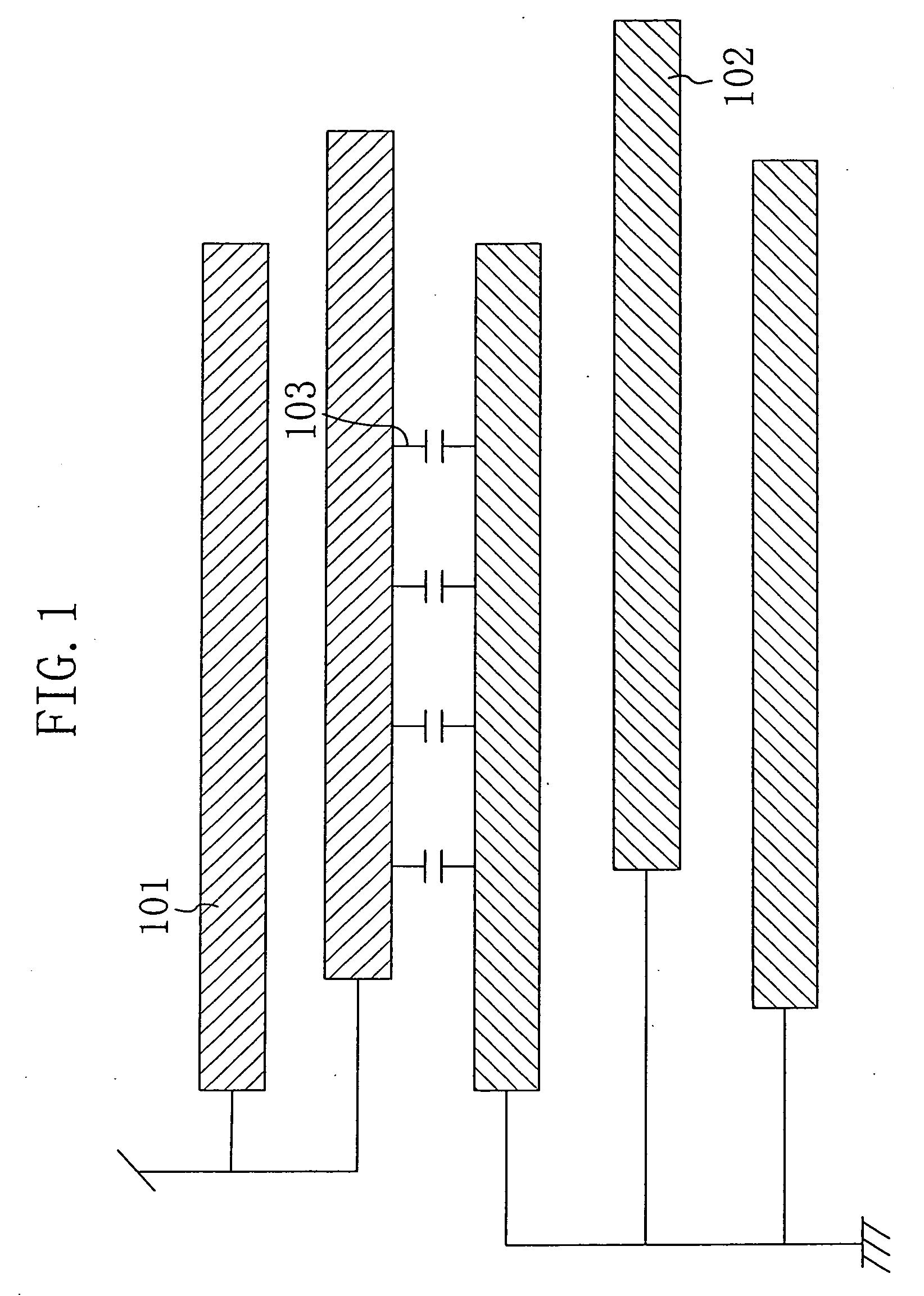
[0046]FIG. 1 is a diagram showing a semiconductor device according to a first embodiment of the present invention. As shown in FIG. 1, the semiconductor device of this embodiment represents an LSI and includes a dummy metal line 101 connected to a power voltage supply unit (VDD) and formed in a first wiring layer (hereinafter, referred to as “upper-wiring-layer dummy metal line 101”) and a dummy metal line 102 connected to the ground (VSS) and formed in a second wiring layer (hereinafter, referred to as “lower-wiring-layer dummy metal line 102”). In this case, the first wiring layer is formed on or above the second wiring layer, and a wiring capacitance 103 is formed between respective regions of the upper-wiring-layer dummy metal line 101 and the lower-wiring-layer dummy metal line 102 overlapping with each other when viewed in a plane. When the first wiring layer is located immediately on the second wiring layer, the wiring capacitance 103 becomes largest. Otherwise, one or more w...
embodiment 2
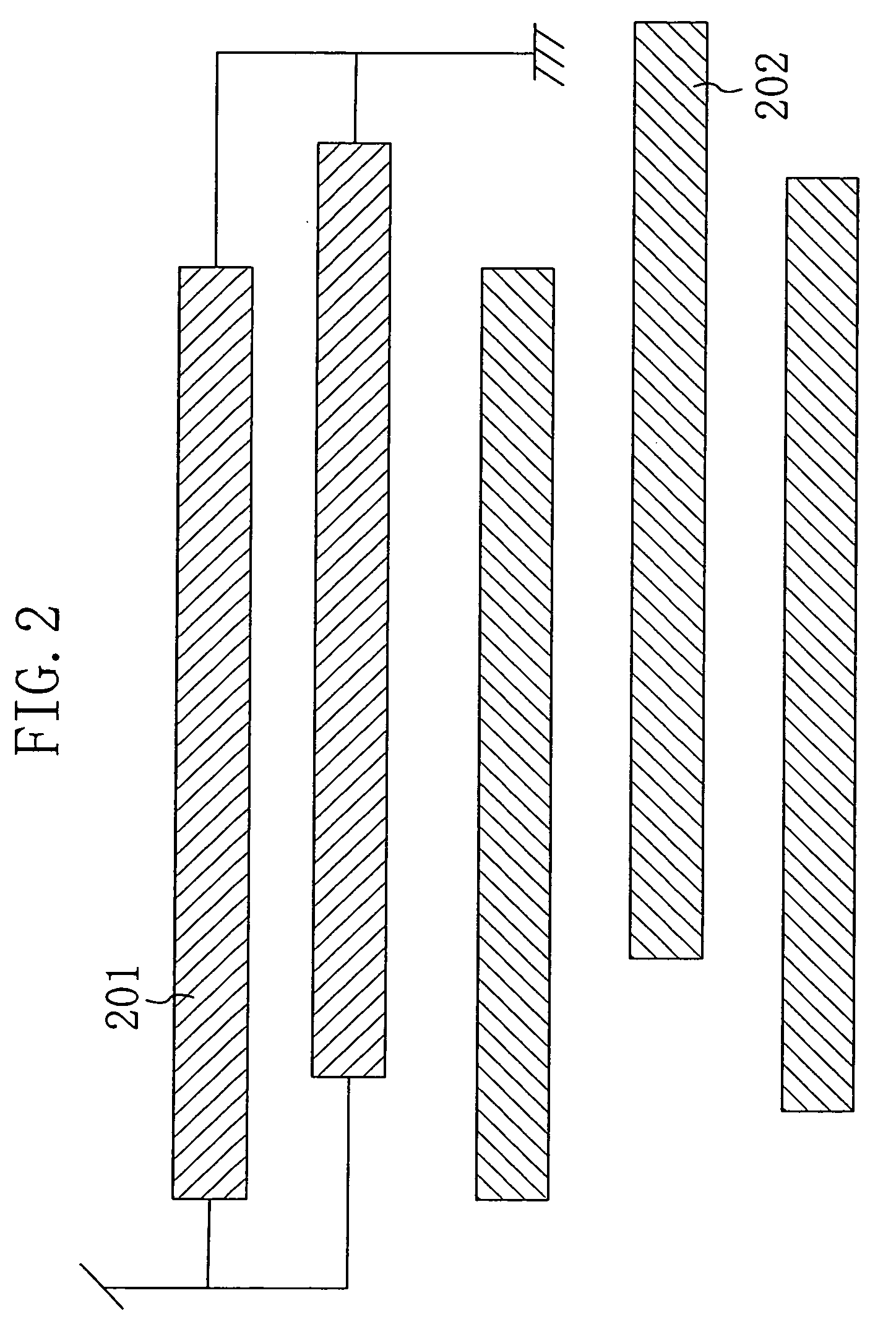
[0053]FIG. 2 is a diagram showing a semiconductor device according to a second embodiment of the present invention. As shown in FIG. 2, the semiconductor device of this embodiment represents an LSI and includes a dummy metal line 201 connected at its two or more points to a power voltage supply unit (VDD) or the ground (VSS) and formed in a first wiring layer (hereinafter, referred to as “upper-wiring-layer dummy metal line 201”) and a dummy metal line 202 isolated from the power voltage supply unit and the ground and formed in a second wiring layer (hereinafter, referred to as “lower-wiring-layer floating-node dummy metal line 202”). When the upper-wiring-layer dummy metal line 201 is formed, it is connected to one of the power voltage supply unit and the ground to which it is more easily connected. Furthermore, the floating-node dummy metal line 202 is formed in a wiring layer in which no power supply line is formed. The other structure is similar to the semiconductor device of th...
embodiment 3
[0056]FIG. 3 is a diagram showing a semiconductor device according to a third embodiment of the present invention. As shown in FIG. 3, the semiconductor device of this embodiment represents an LSI and includes a dummy metal line 301 connected to a power voltage supply unit (VDD) and located in a first wiring layer (hereinafter, referred to as “first upper-wiring-layer dummy metal line 301”), a dummy metal line 302 connected to the ground (VSS) and formed in a different wiring layer (for example, a second wiring layer) from that of the first upper-wiring-layer dummy metal line 301 (hereinafter, referred to as “second upper-wiring-layer dummy metal line 302”), and a dummy metal line 303 isolated from the power voltage supply unit and the ground and formed in a second wiring layer (hereinafter, referred to as “lower-wiring-layer floating-node dummy metal line 303”). In this example, the first wiring layer is formed on the second wiring layer. A wiring capacitance 304 is produced betwee...
PUM
 Abstract
Description
Claims
Application Information
 - R&D Engineer
- R&D Manager
- IP Professional
- Industry Leading Data Capabilities
- Powerful AI technology
- Patent DNA Extraction
Browse by: Latest US Patents, China's latest patents, Technical Efficacy Thesaurus, Application Domain, Technology Topic.
© 2024 PatSnap. All rights reserved.Legal|Privacy policy|Modern Slavery Act Transparency Statement|Sitemap