
Charge transfer device

a technology of charge transfer and discharge device, which is applied in the direction of radiation control devices, semiconductor devices, electrical apparatus, etc., can solve the problems of transfer failure, ccd discharge capacity reduction, and more likely, and achieve the effect of lowering power source voltage and channel potential

Inactive Publication Date: 2008-10-02
NEC ELECTRONICS CORP
View PDF5 Cites 1 Cited by
  • Summary
  • Abstract
  • Description
  • Claims
  • Application Information

AI Technical Summary

Benefits of technology

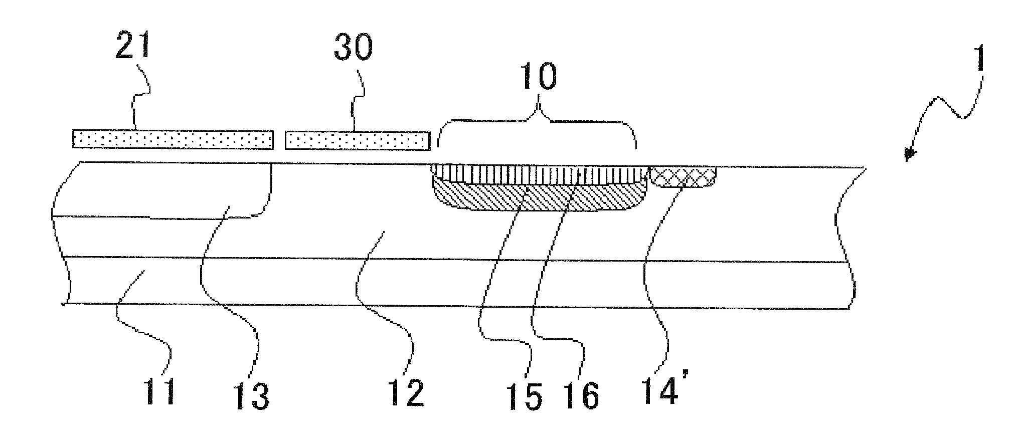
[0019]In this charge transfer device, the storage electrode has P-type conductivity. By virtue of this configuration, channel potential may be lowered (shallower), and thereby power source voltage may be lowered.

Problems solved by technology

However, lower NW concentration makes surface interference more likely to occur, raises a need of adjusting the potential of portions under the barrier electrode at a deeper level, and consequently results in a problem of reduction in maximum charge storage capacity of CCD.
In the surface limit state, electric charge is trapped at the interface between the N-type well and the oxide film in the process of charge transfer, so-called surface interference may occur, and this results in transfer failure.
Accordingly, lower NW concentration makes the surface interference more likely to occur even when the clock voltage in the process of transfer is left unchanged, so that potential under the barrier electrodes need be adjusted to a deeper level, but this consequently reduces the maximum charge storage capacity of CCD.

Method used


Image

  • Charge transfer device
  • Charge transfer device
  • Charge transfer device

Examples


first embodiment

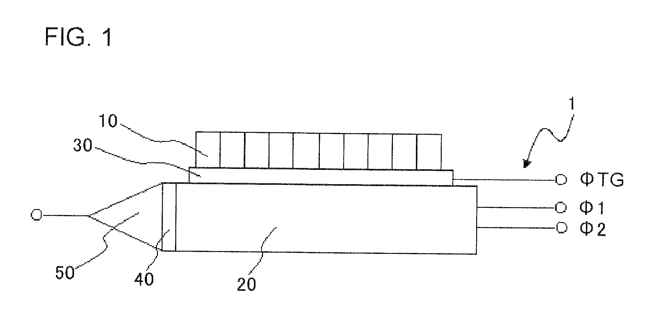
[0042]FIG. 1 is a schematic drawing of a CCD image sensor (charge transfer device) according to a first embodiment of the present invention. A CCD image sensor 1 has photodiodes 10, a CCD register 20, and a transfer gate electrode 30. On one end of the CCD register 20, there are provided a charge detecting unit 40 and an output circuit 50. The transfer gate electrode 30 is provided between the photodiodes 10 and the CCD register 20.

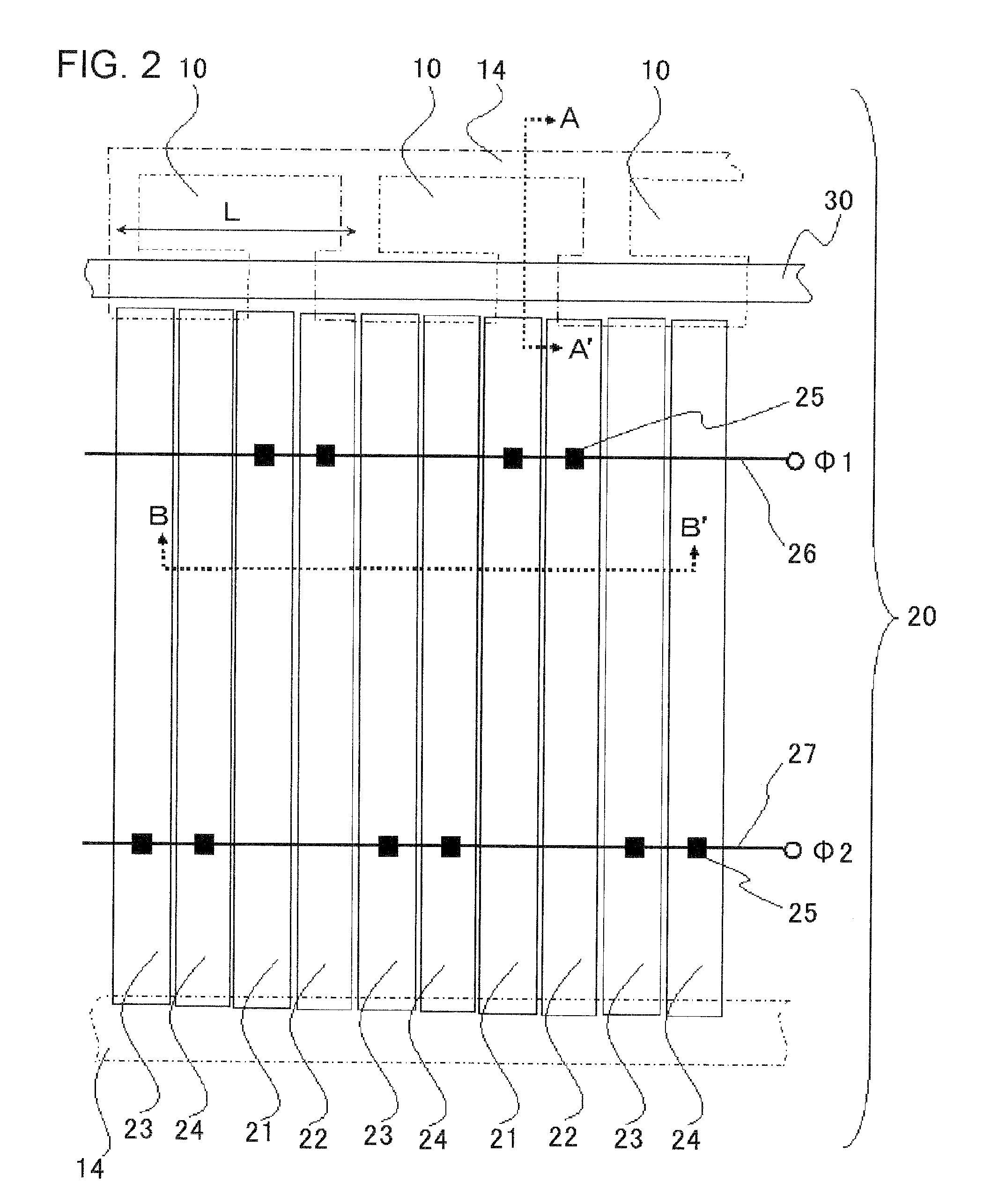
[0043]FIG. 2 is a plan view of a CCD image sensor 1. The photodiodes 10 are isolated from each other by a device isolation region 14 formed of a P+-type diffusion layer, for example. The CCD register 20 contains four types of electrodes 21 to 24. The electrodes 21 are Φ1 storage electrodes. The electrodes 22 are Φ1 barrier electrodes. The electrodes 23 are Φ2 storage electrodes. The electrodes 24 are Φ2 barrier electrodes. These electrodes 21 to 24 are repetitively arranged in this order. The electrodes 21 to 24 are connected via contacts 25 to metal inte...

second embodiment

[0060]FIG. 7 is a plan view of a CCD image sensor according to a second embodiment of the present invention. FIG. 8A and FIG. 8B are sectional views respectively taken along E-E′ and line F-F′ in FIG. 7.

[0061]As shown in FIG. 7, two types of electrodes are arranged in the CCD register. Electrodes 29 are Φ1 electrodes formed of P-type polysilicon. Barrier regions 19 are N−-type diffusion layers formed by ion implantation into the N well under the electrodes 29. Electrodes 28 are Φ2 electrodes formed of P-type polysilicon. Barrier regions 18 are N−-type diffusion layers formed by ion implantation into the N well under the electrodes 28. The electrodes 29, 28 are connected via contacts 25 to metal interconnects 26, 27, respectively, and are supplied with drive pulse Φ1 or Φ2. Assuming now pitch of unit cell in the direction of electron transfer as L, the configuration herein is such as making two electrodes 29 and 28 corresponded to L.

[0062]FIGS. 9A and 9B are a timing chart of drive p...


PUM


Abstract

A charge transfer device 1 has an P-type region, an N-type well provided to the surficial portion of the P-type region, and transfer electrodes having P-type conductivity, provided over the N-type substrate while placing an insulating film in between.

Description

[0001]This application is based on Japanese patent application No. 2007-091330 the content of which is incorporated hereinto by reference.BACKGROUND[0002]1. Technical Field[0003]The present invention relates to a charge transfer device.[0004]2. Related Art[0005]FIG. 10 is a schematic drawing showing a linear CCD (charge coupled device) image sensor of related art. A CCD image sensor 101 has photodiodes 110, a CCD register 120, and a transfer gate electrode 130. On one end of the CCD register 120, there are provided a charge detecting unit 40 and an output circuit 50. The transfer gate electrode 130 is provided between the photodiodes 110 and the CCD register 120.[0006]FIG. 11 is a plan view showing a region in the vicinity of the photodiodes, the transfer gate electrode and the CCD register in the CCD image sensor 101. The photodiodes 110 are isolated from each other by a device isolation region 114 formed of a P+-type diffusion layer.[0007]The CCD register 120 contains four types o...

Claims


Application Information

Patent Timeline
Patent Type & Authority Applications(United States)
IPC IPC(8): H01L29/762
CPCH01L27/14806H01L29/76833
Inventor MATSUYAMA, EIJI
Owner NEC ELECTRONICS CORP
Learn More