Current source circuit and method of outputting current
a current source circuit and output current technology, applied in the direction of electric variable regulation, process and machine control, instruments, etc., can solve the problems of not being able to determine the ratio of current ability and color difference on display
- Summary
- Abstract
- Description
- Claims
- Application Information
AI Technical Summary
Benefits of technology
Problems solved by technology
Method used
Image

Examples
first embodiment
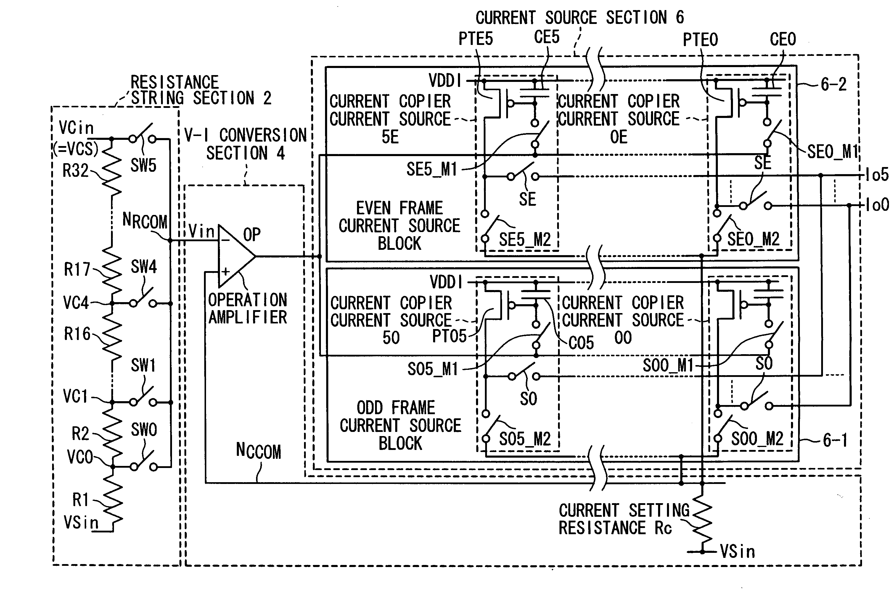
[0087]As shown in FIG. 10, the current source circuit according to the first embodiment of the present invention is composed of a resistance string section 2, a V-I conversion section 4, and a current source section 6.
[0088]The resistance string section 2 is composed of 32 resistances R1, R2, . . . , R32, and six switches SW0, SW1, SW2, . . . SW5. The switches are supplied with control signals which are given the same names as the switches. The 32 resistances have a same resistance value and are connected in series. Voltages VCin (VCS) and VSin are applied across both ends of the resistance string. Each of the six switches is connected at one end with a common node NRCOM as an output of the resistance string section 2 to output a voltage Vin. The other end of each of the six switches is connected with one of a node between the resistances R1 and R2 (VC0), a node between the resistances R2 and R3 (VC1), a node between the resistances R4 and R5 (VC2), a node between the resistances R8...
second embodiment
[0109]The circuit structure of the current source circuit according to the second embodiment will be described with reference to FIG. 13. In the first embodiment, when the operation amplifier OP in the V-I conversion section has an offset voltage Voff, the output current Ii sometimes shifts by the offset voltage, for example, to I5=(VCin+Voff−VSin) / Rc. In this case, this current ratio is different from an ideal current ratio. In the second embodiment, an offset cancellation block is added to the V-I conversion section in the first embodiment.
[0110]The offset cancellation block has a capacitance and switches. The resistance string section 2 and the current source section 6 in the second embodiment are the same as those of the first embodiment.
[0111]As shown in FIG. 13, the V-I conversion section 4A in the second embodiment is composed of the operation amplifier OP, the current setting resistance Rc, a capacitance Coc, and switches OC1, OC1B and OC2. The output of the resistance strin...
third embodiment
[0123]The current source circuit according to the third embodiment can cancel an offset voltage of the operation amplifier OP even when the offset voltage of the operation amplifier OP in the V-I conversion section 4A of the second embodiment is large. The circuit structure in the third embodiment is shown in FIG. 16 and an operation of the structure is shown in the timing chart of FIGS. 17A to 17M.
[0124]The third embodiment basically has the same circuit structure and operation as those of the second embodiment. However, the switch OC1B is replaced by a switch / OC1. Also, one end of the current setting resistance Rc on the opposite side of the node NCCOM is connected with the voltage Vsin via a switch / OC1 and a voltage VL via a switch OC1. The switches OC1 are turned on in response to the control signal OC1 and the switches / OC1 are turned on in response to the control signal / OC1 which is an inverted signal of the control signal OC1.
[0125]In the third embodiment, the voltage VSin is...
PUM
 Abstract
Description
Claims
Application Information
 - R&D
- Intellectual Property
- Life Sciences
- Materials
- Tech Scout
- Unparalleled Data Quality
- Higher Quality Content
- 60% Fewer Hallucinations
Browse by: Latest US Patents, China's latest patents, Technical Efficacy Thesaurus, Application Domain, Technology Topic, Popular Technical Reports.
© 2025 PatSnap. All rights reserved.Legal|Privacy policy|Modern Slavery Act Transparency Statement|Sitemap|About US| Contact US: help@patsnap.com