Method for forming amorphouse silicon film by plasma CVD

a technology of amorphous silicon and plasma cvd, which is applied in the direction of coating, chemical vapor deposition coating, metallic material coating process, etc., can solve the problems of foreign substances being produced, the uniformity of in-plane film thickness is deteriorated, and it is difficult to improve the film stress and uniformity of in-plane film thickness at the same time, so as to improve the film stress and improve the film stress.

Inactive Publication Date: 2008-12-04
ASM JAPAN
View PDF7 Cites 16 Cited by
  • Summary
  • Abstract
  • Description
  • Claims
  • Application Information

AI Technical Summary

Benefits of technology

[0006]The present invention provides a new method for controlling the film stress of an amorphous silicon film. In an embodiment of the present invention, the film stress of an amorphous silicon film is controlled over a wide range only by means of the flow rate of the source gas, flow rate of the dilution gas, and film forming pressure, without using any additive gas. In general, a low film stress (“low film stress” means that the absolute stress value is small, and does not mean that the negative value of compressive stress is large) leads to deterioration in the uniformity of in-plane film thickness, which makes it difficult to improve both the film stress and uniformity of in-plane film thickness at the same time. By using the aforementioned control method, however, the in-plane uniformity can be adjusted by controlling the flow rate of the source gas, flow rate of the dilution gas, and film forming pressure. Furthermore, the flow rate of the source gas, flow rate of the dilution gas, and film forming pressure can be used as control parameters to improve the film stress without changing the uniformity of in-plane film thickness that has already been optimized.

Problems solved by technology

In general, a low film stress (“low film stress” means that the absolute stress value is small, and does not mean that the negative value of compressive stress is large) leads to deterioration in the uniformity of in-plane film thickness, which makes it difficult to improve both the film stress and uniformity of in-plane film thickness at the same time.
Such discharge at the upper electrode can cause production of foreign substances.

Method used


Image

  • Method for forming amorphouse silicon film by plasma CVD
  • Method for forming amorphouse silicon film by plasma CVD
  • Method for forming amorphouse silicon film by plasma CVD

Examples


examples

[0055]The present invention will be explained with reference to preferred examples and drawings. However, the examples and drawings are not intended to limit the present invention.

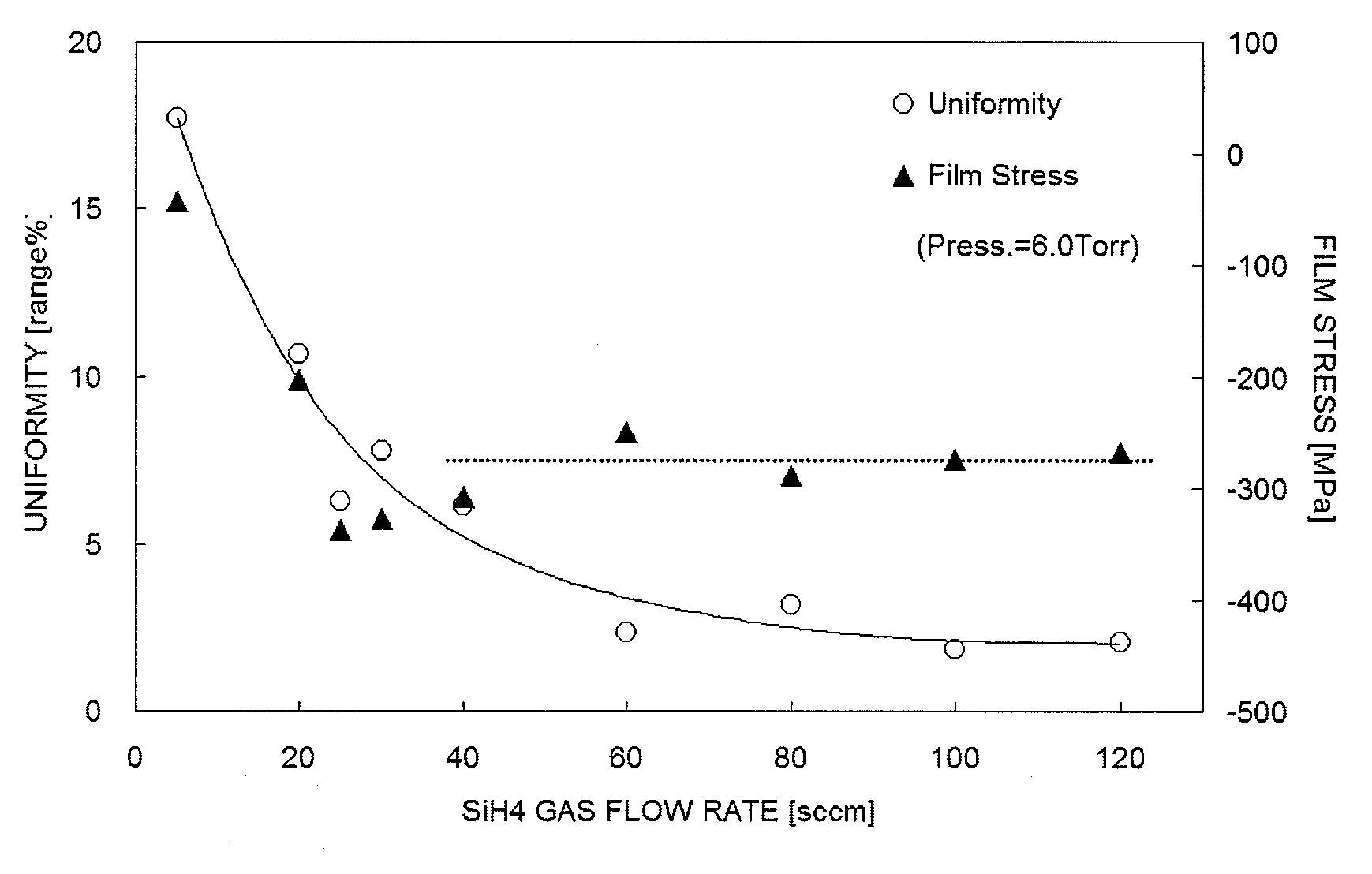
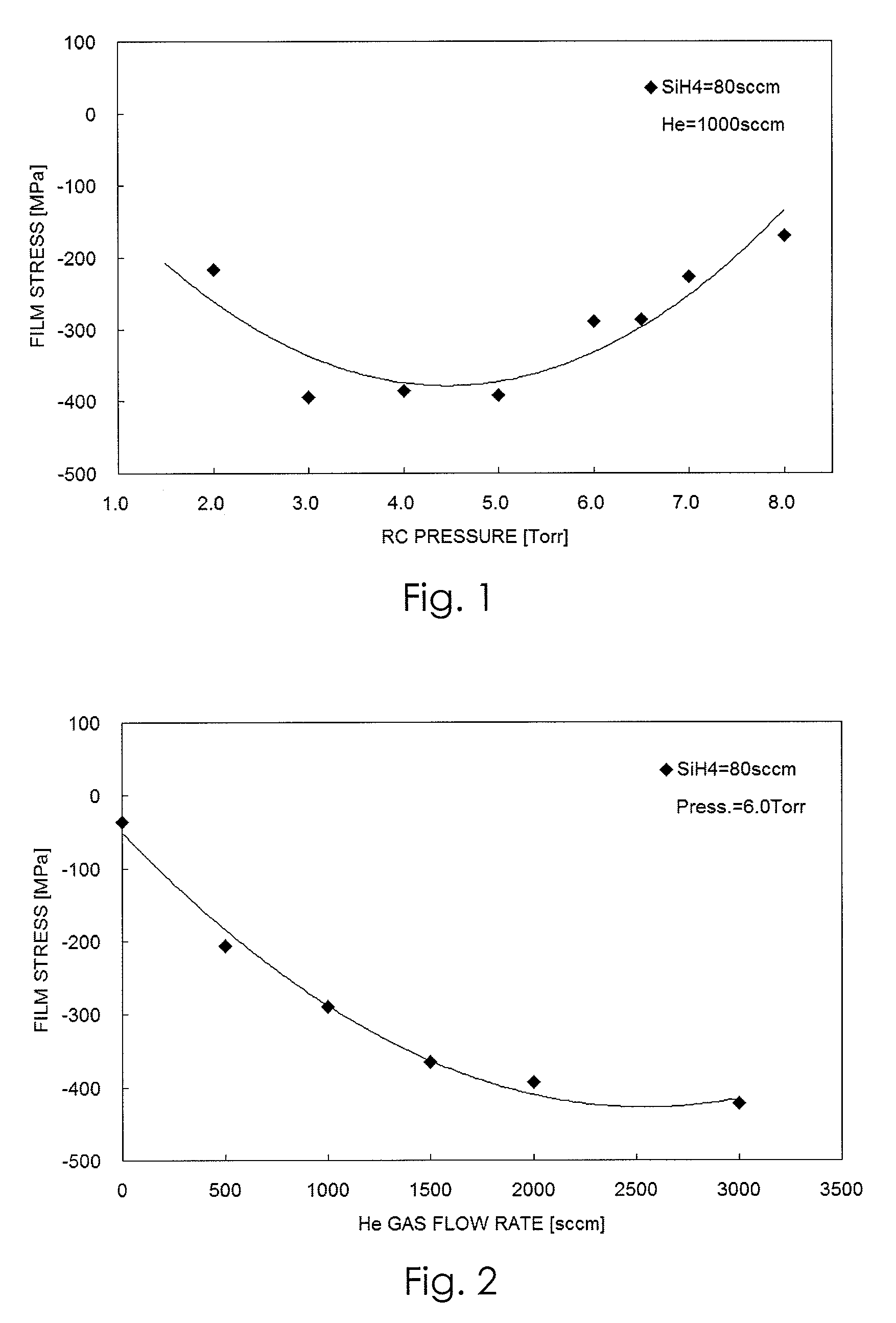
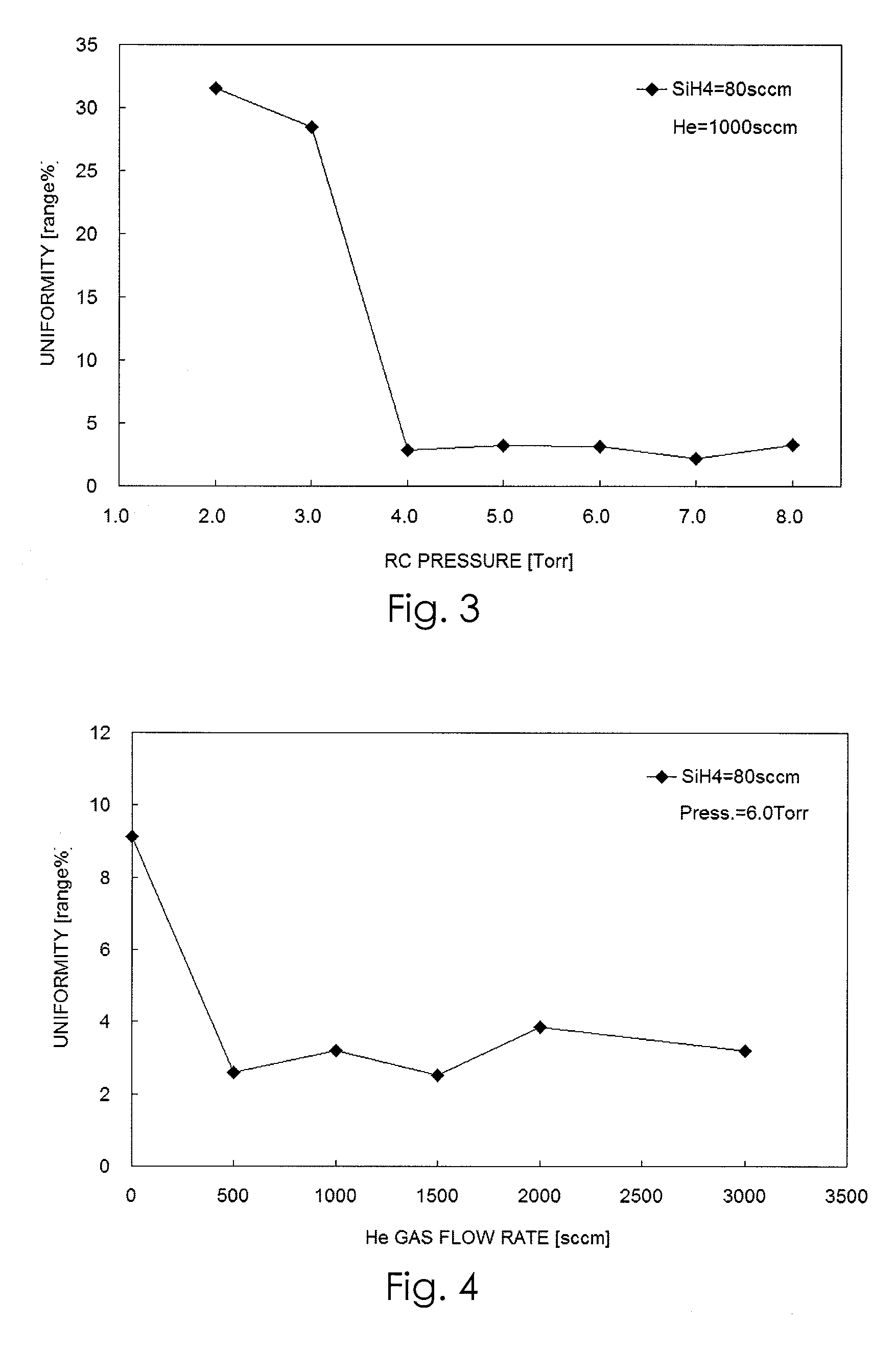
[0056]The best mode for carrying out the present invention is explained below by referring to Tables 1 and 3, and FIGS. 1 through 5. It is clear that, by forming an amorphous silicon film under the ranges of conditions shown in Table 1 and without using any separate additive gas, it becomes possible to control the film stress of the obtained film over a wide range. For your reference, other conditions used in the examples described below are shown in Table 3. Eagle® 12 manufactured by ASM Japan K.K. was used as the apparatus.

TABLE 1SiH4 / sccmHe / slmPressure / Torr5~1200.0~3.02.0~8.0

TABLE 2WallRFLowerUppertem-DistanceFilmfre-RFelec-elec-pera-betweenthick-quencypowertrodetrodetureelectrodesness13.56 MHz450 W600° C.155° C.140° C.14 mm100 nm

[0057]FIG. 1 shows how the film stress changes with respect to the film fo...


PUM

PropertyMeasurementUnit
compressiveaaaaaaaaaa
pressureaaaaaaaaaa
pressureaaaaaaaaaa

Abstract

A method includes introducing a silicon-containing source gas and a dilution gas to a reactor to deposit an amorphous silicon film on a substrate by plasma CVD; and adjusting a compressive film stress to 300 MPa or less and a uniformity of film thickness within the substrate surface to ±5% or less of the amorphous silicon film depositing on the substrate as a function of a flow rate of the source gas, a flow rate of the dilution gas, and a pressure of the reactor which are used as control parameters.

Description

BACKGROUND OF THE INVENTION[0001]1. Field of the Invention[0002]The present invention generally relates to a method for forming an amorphous silicon film by plasma CVD having a low compressive film stress and a high uniformity of film thickness.[0003]2. Description of the Related Art[0004]Amorphous silicon films are widely used as intermediate films in semiconductor processes, such as the manufacturing process for thin film transistors (TFT) and the production of field emission displays (FED) for liquid crystal devices. In recent years, amorphous silicon films are also finding a promising application as hard masks for metal gates in the dual-metal gate process. In this integration process, the step in which the first metal is etched requires that metal be removed completely without damaging the high-k insulation film, while the step in which the hard mask is removed calls for a certain selection ratio between the underlying metal and high-k insulation film. Amorphous silicon films a...

Claims


Application Information

Patent Timeline
Patent Type & Authority Applications(United States)
IPC IPC(8): H01L21/20
CPCC23C16/24C23C16/52H01L21/02532H01L21/02592H01L21/0262
Inventor ARAI, HIROFUMIWATANABE, TAKASHIGE
Owner ASM JAPAN
Why Eureka
Try Eureka