Method for increasing film stress and method for forming high stress layer

a film stress and high-stress technology, which is applied in the direction of basic electric elements, electrical equipment, semiconductor devices, etc., can solve the problems of bombarding power consumption, insufficient stress value required by process of 65 nm or below, and thin film deposition technology presently used in the industry cannot meet the requirements of ic process, etc., to achieve plasma-enhanced chemical vapor deposition, increase film stress, and increase film stress

Inactive Publication Date: 2008-07-03
UNITED MICROELECTRONICS CORP
View PDF9 Cites 3 Cited by
  • Summary
  • Abstract
  • Description
  • Claims
  • Application Information

AI Technical Summary

Benefits of technology

[0008]Accordingly, the present invention is directed to provide a method for increasing film stress, which can prevent the collision between the gas atoms in a plasma-enhanced chemical vapor deposition (PECVD) operation from affecting the efficiency of deposition and can increase the film stress.

Problems solved by technology

Generally speaking, the thin film deposition technology presently used in the industry cannot meet the requirement of IC process.
It is provided by the industry that an inert gas of greater molecular weight is added into conventional PECVD technology to increase the stress of the deposited film up to about −2.4 GPa, however, this is still not sufficient for the stress value required by process of 65 nm or below.
Besides, since a gas of greater molecular weight is added for increasing the film stress in deposition process, bombard power consumption may be caused and the deposition efficiency is reduced due to the collisions between the gas atoms and the collisions of the gas with the nitrogen carrier gas used in conventional PECVD technology.

Method used


Image

  • Method for increasing film stress and method for forming high stress layer
  • Method for increasing film stress and method for forming high stress layer

Examples


Embodiment Construction

[0025]Reference will now be made in detail to the present preferred embodiments of the invention, examples of which are illustrated in the accompanying drawings. Wherever possible, the same reference numbers are used in the drawings and the description to refer to the same or like parts.

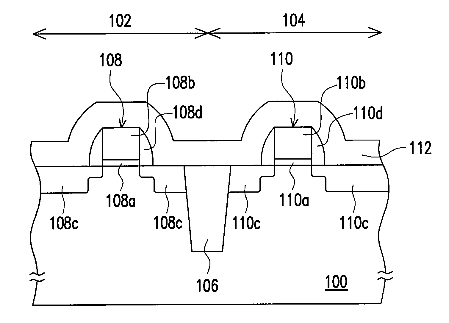
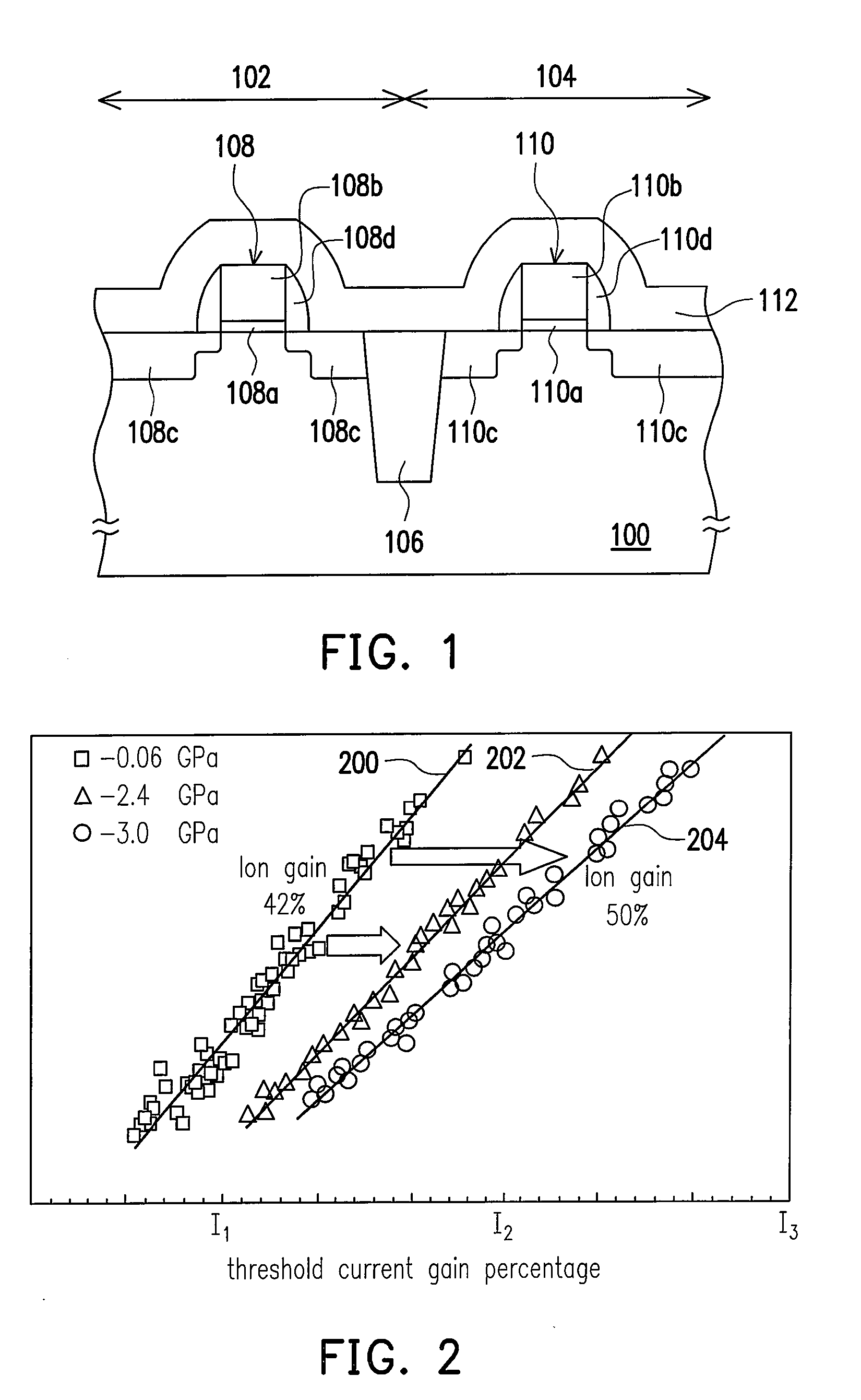
[0026]In the manufacturing process of IC device, the driving current of a device can be improved effectively by increasing the stress of the shallow trench isolation oxide (STI Oxide) layer, the polysilicon cap silicon nitride (Poly-cap SiN) layer, and the contact silicon nitride stop layer film etc.

[0027]A stress of the film is increased by the methods in the present invention so as to form a high stress layer, and can improve the performance of the device accordingly. Below, the present invention will be described with the example of forming a high compressive stress silicon nitride layer.

[0028]Generally, before the PECVD process is performed, a pre-gas is added into the reactor to reach the pressu...


PUM


Abstract

A method for forming a high stress layer is provided. According to the method, a substrate is put into a reactor of a PECVD machine and a reaction gas is added into the reactor. Then, an assistant reaction gas which has the molecular weight greater than or equal to the molecular weight of nitrogen gas is added into the reactor. Next, a carrier gas which has the molecular weight smaller than the molecular weight of nitrogen gas is added into the reactor to increase the bombarding efficiency in film deposition. Thereby, the high stress layer is formed on the substrate.

Description

BACKGROUND OF THE INVENTION[0001]1. Field of the Invention[0002]The present invention relates to a method for forming a stress layer. More particularly, the present invention relates to a method for increasing film stress and a method for forming a high stress layer.[0003]2. Description of Related Art[0004]Along with semiconductor fabricating process entering an era of deep submicron, increasing the driving current of NMOS device and PMOS device has been more and more focused on. In particular, as to the process beyond present 65 nm, time delay and operation rate of the device can be improved considerably by increasing the driving current of NMOS and PMOS effectively.[0005]Recently, various methods for increasing device driving current using internal stress have been provided in the industry, wherein the methods include increasing stress of shallow trench isolation oxide (STI Oxide), polysilicon cap silicon nitride (Poly-cap SiN) layer, and contact silicon nitride stop layer film et...

Claims


Application Information

Patent Timeline
Patent Type & Authority Applications(United States)
IPC IPC(8): H01L21/469
CPCH01L21/3185H01L29/7843H01L21/823807
Inventor CHEN, NENG-KUOTSAI, TENG-CHUNHUANG, CHIEN-CHUNG
Owner UNITED MICROELECTRONICS CORP
Why Eureka
Try Eureka