Semiconductor substrate cleaning method using bubble/chemical mixed cleaning liquid

a technology of semiconductor substrates and cleaning liquids, applied in the field of cleaning processes, can solve the problems of reducing particle removal efficiency, and affecting the cleaning effect of semiconductor substrates

Inactive Publication Date: 2008-12-18
KK TOSHIBA
View PDF4 Cites 14 Cited by
  • Summary
  • Abstract
  • Description
  • Claims
  • Application Information

AI Technical Summary

Benefits of technology

[0034]FIG. 12 schematically shows the configuration of a conventional bubble generator.

Problems solved by technology

However, in the MHz and two-fluid jet cleaning methods, there is a strong correlation between the particle removal efficiency and the incidence of defects in the device pattern.
That is, with higher power, the particle removal efficiency increases, but the possibility that the pattern will be damaged becomes stronger.
In contrast, under a low-power condition that prevents the pattern from being damaged, the particle removal efficiency decreases and the fabrication yield cannot be increased as much as expected.
Furthermore, in the semiconductor devices of the 50-nm generation and afterward, since the pattern size is smaller than the size of particles to be removed, cleaning becomes more difficult than now; therefore, it is expected that manufacturing devices in a high yield will become very difficult.
However, depending on the underlaying material that has adsorbed particles, the alkali cleaning method cannot be applied.
However, with a conventional in-liquid bubble generator, it is difficult to generate bubbles of several nanometers in size stably.
Furthermore, when bubbles are generated in a liquid, since the bubbles continue growing very big until bubbles have desorbed from the bubble generating region due to buoyancy in the liquid, it is difficult to generate nano-sized bubbles.

Method used


Image

  • Semiconductor substrate cleaning method using bubble/chemical mixed cleaning liquid
  • Semiconductor substrate cleaning method using bubble/chemical mixed cleaning liquid
  • Semiconductor substrate cleaning method using bubble/chemical mixed cleaning liquid

Examples


first embodiment

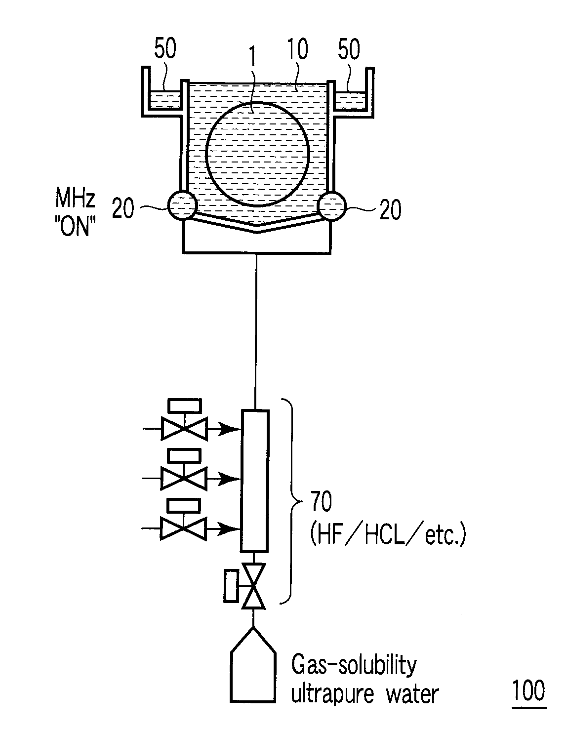
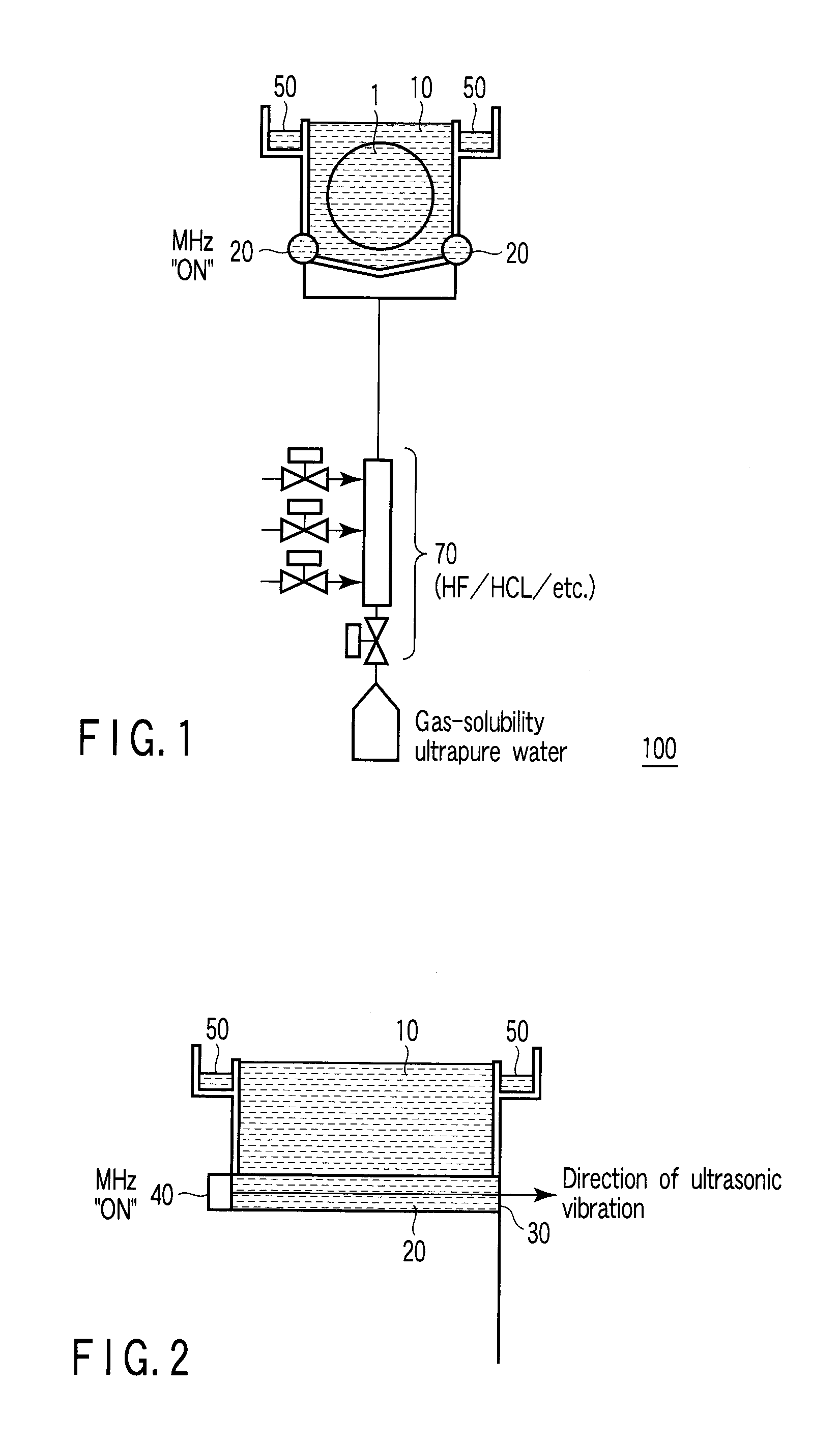
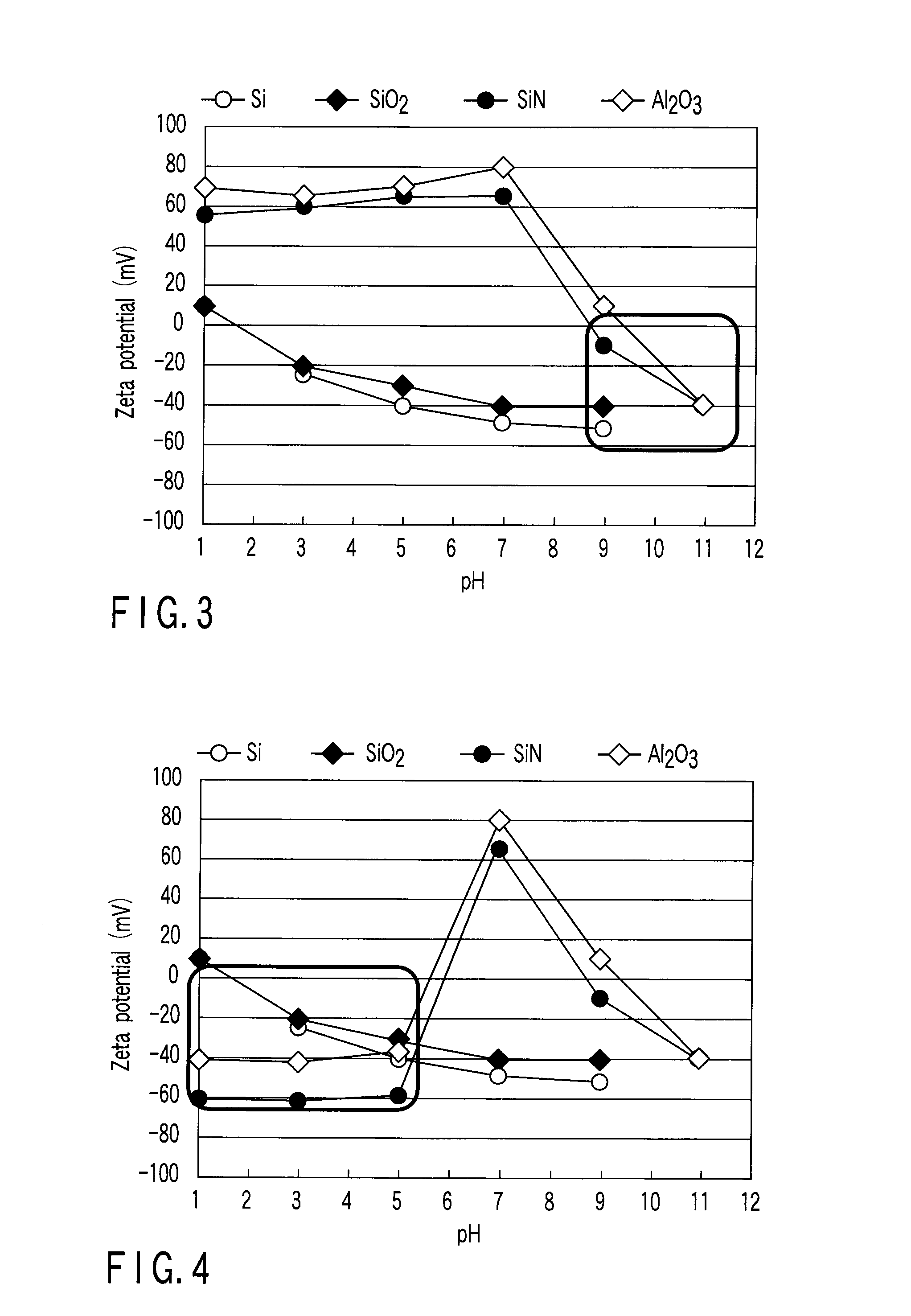
[0035]A semiconductor substrate cleaning method according to a first embodiment of the invention will be explained using FIGS. 1 to 5. In the first embodiment, ultrasonic waves are applied to a chemical in which gas is dissolved to a saturated concentration, thereby generating bubbles. Using a bubble / chemical mixed cleaning liquid, the semiconductor substrate is cleaned.

[0036]FIGS. 1 and 2 show a one-bath batch cleaning apparatus 100 as an example of a semiconductor substrate cleaning apparatus which carries out a semiconductor substrate cleaning method according to the first embodiment. FIG. 1 is a schematic configuration diagram and FIG. 2 is a sectional view taken in a direction perpendicular to the sheet of paper of FIG. 1.

[0037]As shown in FIGS. 1 and 2, a quartz processing bath 10 is filled with a chemical acting as a cleaning liquid. In the chemical, a wafer (semiconductor substrate) 1 is immersed. Chemical supply quartz tubes 20, which are for supplying the chemical to the q...

second embodiment

[0059]A semiconductor substrate cleaning method according to a second embodiment of the invention will be explained using FIGS. 6 and 7. In the second embodiment, using a bubbler (bubble generator), bubbles are generated in a chemical in which gas have been dissolved to the saturated concentration. Using a bubble / chemical mixed cleaning liquid, a semiconductor substrate is cleaned.

[0060]FIG. 6 shows a circulation batch cleaning apparatus 600 as an example of a semiconductor substrate cleaning apparatus which carries out a semiconductor substrate cleaning method according to the second embodiment. A chemical, which circulates through a circulation pipe 64, passes through a pump 61, a heater 62, and a filter 63. At a bubbler (bubble generator) 60, nitrogen (N2) gas is mixed in the chemical, which is then supplied via a chemical supply quartz tube 20 to a quartz processing bath 10. After the cleaning liquid which cleaned a wafer 1 in the processing bath 10 overflows the processing bath...

third embodiment

[0079]Next, a semiconductor substrate cleaning method according to a third embodiment of the invention will be explained using FIGS. 8A and 8B. In the third embodiment, a semiconductor substrate is cleaned using a bubble-mixed liquid in a two-fluid jet cleaning method using two fluids, liquid and gas.

[0080]In a rotary drying technique using a sheet-feed cleaning apparatus, a method of supplying a cleaning liquid to a rotating wafer in such a manner that the liquid is sprayed to the center of the wafer and a method of supplying a cleaning liquid to the wafer from a scan nozzle can be used. Both methods are generally used in a sheet-feed cleaning apparatus.

[0081]The third embodiment is characterized by a method of supplying a chemical. Specifically, as shown in FIG. 8A, a bubble generator 802 is provided on the chemical flow (or purified water flow) 81 supplying side of a jet nozzle (chemical spray nozzle) 800. When a chemical is sprayed from the jet nozzle 800, the chemical flow (or ...


PUM

PropertyMeasurementUnit
gate lengthaaaaaaaaaa
sizeaaaaaaaaaa

Abstract

A method has been disclosed which cleans a semiconductor substrate using a cleaning liquid produced by mixing bubbles of a gas into an acid solution in which the gas has been dissolved to the saturated concentration and which brings the zeta potentials of the semiconductor substrate and adsorbed particles into the negative region by the introduction of an interfacial active agent. Alternatively, a semiconductor substrate is cleaned using a cleaning liquid produced by mixing bubbles of a gas into an alkaline solution in which the gas has been dissolved to the saturated concentration and whose pH is 9 or more.

Description

CROSS-REFERENCE TO RELATED APPLICATIONS[0001]This application is based upon and claims the benefit of priority from prior Japanese Patent Application No. 2007-142199, filed May 29, 2007, the entire contents of which are incorporated herein by reference.BACKGROUND OF THE INVENTION[0002]1. Field of the Invention[0003]This invention relates to a cleaning process in the semiconductor device manufacturing steps, and more particularly to a semiconductor substrate cleaning method using chemical (bubble / chemical mixed cleaning liquid) including bubbles of a nanometer or micrometer size.[0004]2. Description of the Related Art[0005]In recent years, a semiconductor device where MOSFETs with a gate length of 65 nm have been integrated has been developed and commercialized. In the case of the next-generation semiconductor devices whose patterns have been miniaturized further, those whose gate length is 50 nm or less have been developed.[0006]To manufacture semiconductor devices of the 65-nm gene...

Claims


Application Information

Patent Timeline
Patent Type & Authority Applications(United States)
IPC IPC(8): B08B3/12B08B3/08
CPCB08B3/10B08B3/12C11D3/0052C11D11/0047H01L21/02052H01L21/02057H01L21/67057H01L21/304
Inventor TOMITA, HIROSHIIIMORI, HIROYASUYAMADA, HIROAKIINUKAI, MINAKO
Owner KK TOSHIBA
Why Eureka
Try Eureka