Trench gate semiconductor device and method of manufacturing the same

a semiconductor device and clamping gate technology, applied in semiconductor devices, diodes, electrical devices, etc., can solve the problems of forward voltage drop of the aforesaid diode that cannot be neglected as a loss, difficult gate voltage control, and loss of forward voltage drop

Active Publication Date: 2009-03-05
KK TOSHIBA
View PDF7 Cites 65 Cited by
  • Summary
  • Abstract
  • Description
  • Claims
  • Application Information

AI Technical Summary

Problems solved by technology

However, in accordance with an increasing demand for lower voltage as output voltage of the load side, forward voltage drop of the aforesaid diode cannot be neglected as a loss.
In the above-described structure, it is difficult to control gate voltage so as to turn on the second MOS transistor in exactly the same period as the conduction period of the diode, and in actual practice, a period when the chopping MOS transistor and the second MOS transistor both turn off (dead time) is provided.
This period, even though short, also involves a problem of forward voltage drop as a loss.

Method used


Image

  • Trench gate semiconductor device and method of manufacturing the same
  • Trench gate semiconductor device and method of manufacturing the same
  • Trench gate semiconductor device and method of manufacturing the same

Examples


Embodiment Construction

Description of Embodiments

[0016]Embodiments of the present invention will be described with reference to the drawings, but these drawings are provided only for an illustrative purpose and are not to limit the present invention in any respect.

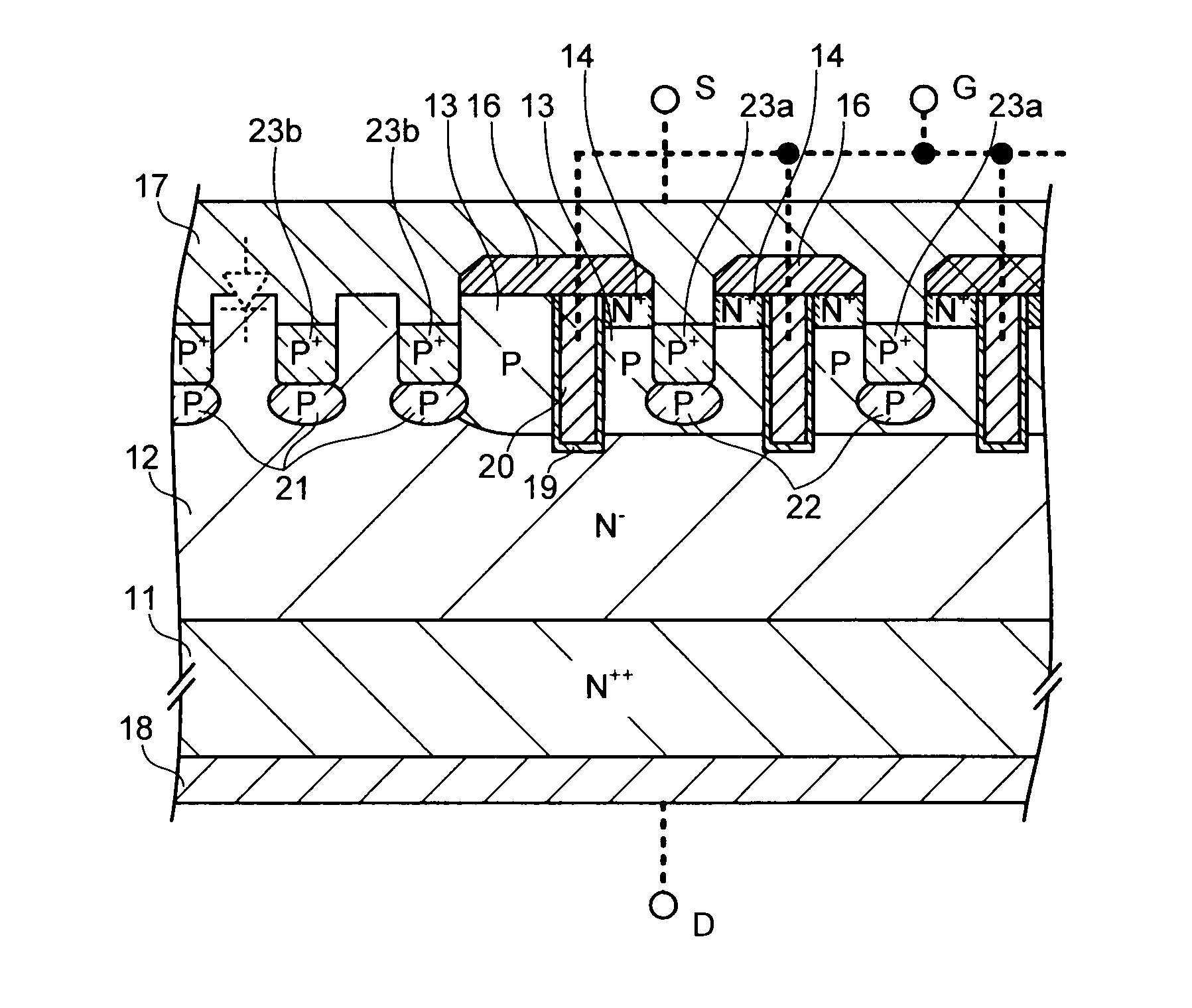
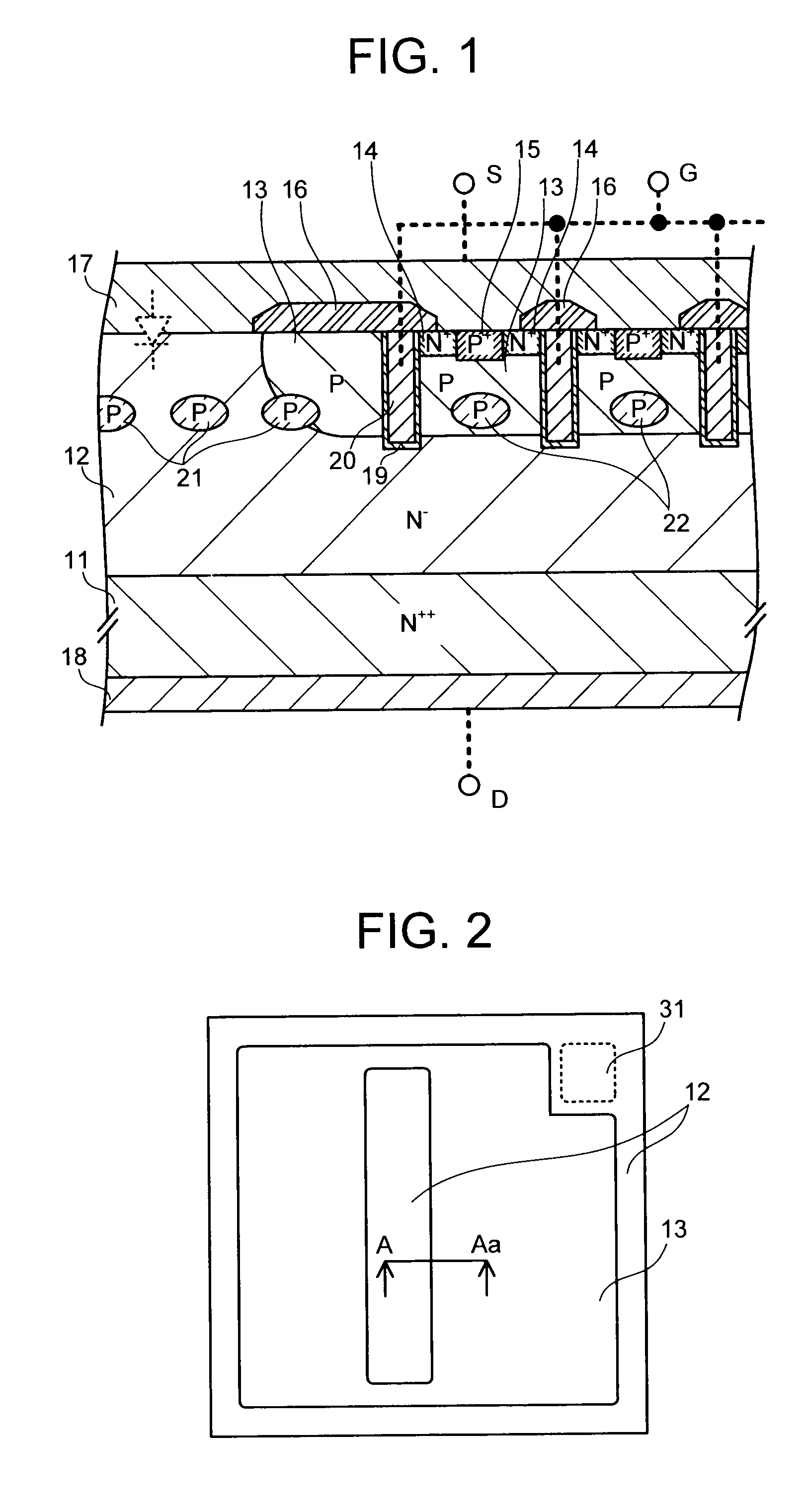
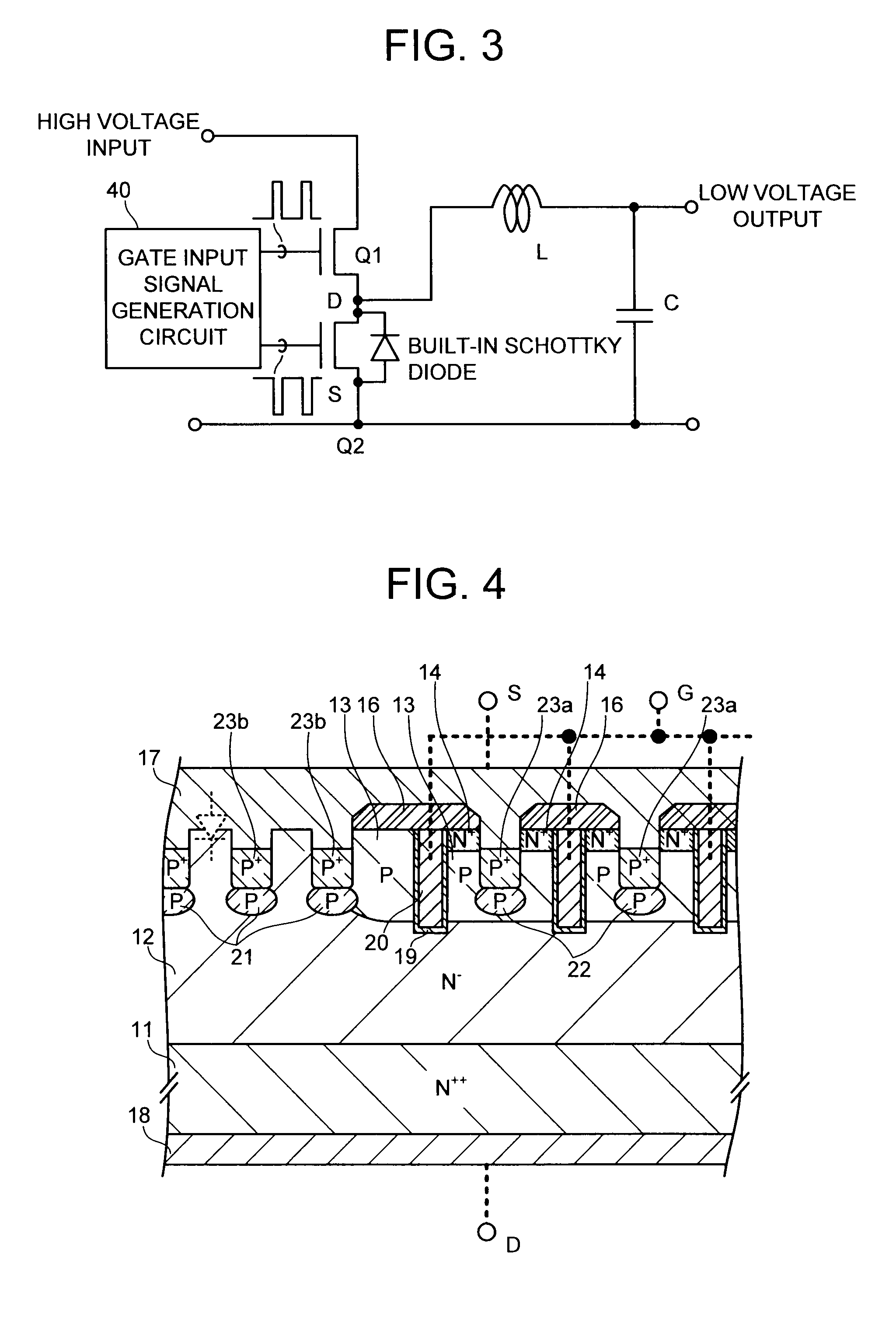
[0017]Hereinafter, the embodiments of the present invention will be described with reference to the drawings. FIG. 1 is a cross-sectional view schematically showing the structure of a trench gate semiconductor device (trench gate MOS transistor, as an example) according to one embodiment of the present invention. In the description here, n-type is defined as a first conductivity type and p-type is defined as a second conductivity type, but the embodiments to be described below can be carried out with these types interchanged. As shown in FIG. 1, the trench gate MOS transistor has an n-type semiconductor substrate 11, an n-type semiconductor layer 12 (drift layer; semiconductor layer of a first conductivity type), a p-type base layer 13 (diffusio...


PUM


Abstract

Disclosed is a trench gate semiconductor device including: a semiconductor layer having a first conductivity type; a first diffusion region having a second conductivity type having a planar structure on the semiconductor layer; a second diffusion region having the first conductivity type positioned selectively on the first diffusion region; a gate electrode provided via a gate insulation film in each first trench facing the second diffusion region and penetrating through the first diffusion region to reach the semiconductor layer; a first semiconductor region of the second conductivity type provided at a position, in the semiconductor layer, apart in a lateral direction from the first diffusion region; a second semiconductor region of the second conductivity type provided at a position, in the first diffusion region, between the adjacent first trenches; and a main electrode in contact with the semiconductor layer and the second diffusion region.

Description

CROSS-REFERENCE TO RELATED APPLICATIONS[0001]This application is based upon and claims the benefit of priority from the prior Japanese Patent Application No. 2007-225414, filed on Aug. 31, 2007; the entire contents of which are incorporated herein by reference.BACKGROUND[0002]1. Field of the Invention[0003]The present invention relates to a trench gate semiconductor device having a gate electrode in a trench formed in a semiconductor region and a method of manufacturing the same, and in particular, to a trench gate semiconductor device in which a Schottky diode is integrally formed in parallel between a source and a drain and a method of manufacturing the same.[0004]2. Description of the Related Art[0005]In a DC-DC converter for voltage step-down, a MOS transistor is used as a switching (chopping) element. In a period during which current passage from a primary side to a secondary side is interrupted by the switching, a reflux structure by a flywheel diode can be useful to prevent t...

Claims


Application Information

Patent Timeline
Patent Type & Authority Applications(United States)
IPC IPC(8): H01L29/78H01L21/336
CPCH01L29/0619H01L29/0623H01L29/0696H01L29/7813H01L29/41766H01L29/7806H01L29/1095
Inventor HOKOMOTO, YOSHITAKAHARA, TAKUMA
Owner KK TOSHIBA
Why Eureka
Try Eureka