Biosensor using nanoscale material as transistor channel and method of fabricating the same

a biosensor and nano-scale material technology, applied in the field of biosensors and methods of fabricating biosensors, can solve the problems of difficult accuracy of collecting and analysing light emitted from fluorescent materials, and the time-consuming and labor-intensive nature of bio-sample fluorescence analysis

Inactive Publication Date: 2009-04-02
SAMSUNG ELECTRONICS CO LTD
View PDF24 Cites 24 Cited by
  • Summary
  • Abstract
  • Description
  • Claims
  • Application Information

AI Technical Summary

Problems solved by technology

However, fluorescent analysis of a bio-sample takes a relatively long period of time because of the steps involved, including marking the bio-sample with fluorescent material and performing the scanning process.
Furthermore, accurately collecting and analyzing the light emitted from the fluorescent material is not easy.

Method used


Image

  • Biosensor using nanoscale material as transistor channel and method of fabricating the same
  • Biosensor using nanoscale material as transistor channel and method of fabricating the same
  • Biosensor using nanoscale material as transistor channel and method of fabricating the same

Examples


Embodiment Construction

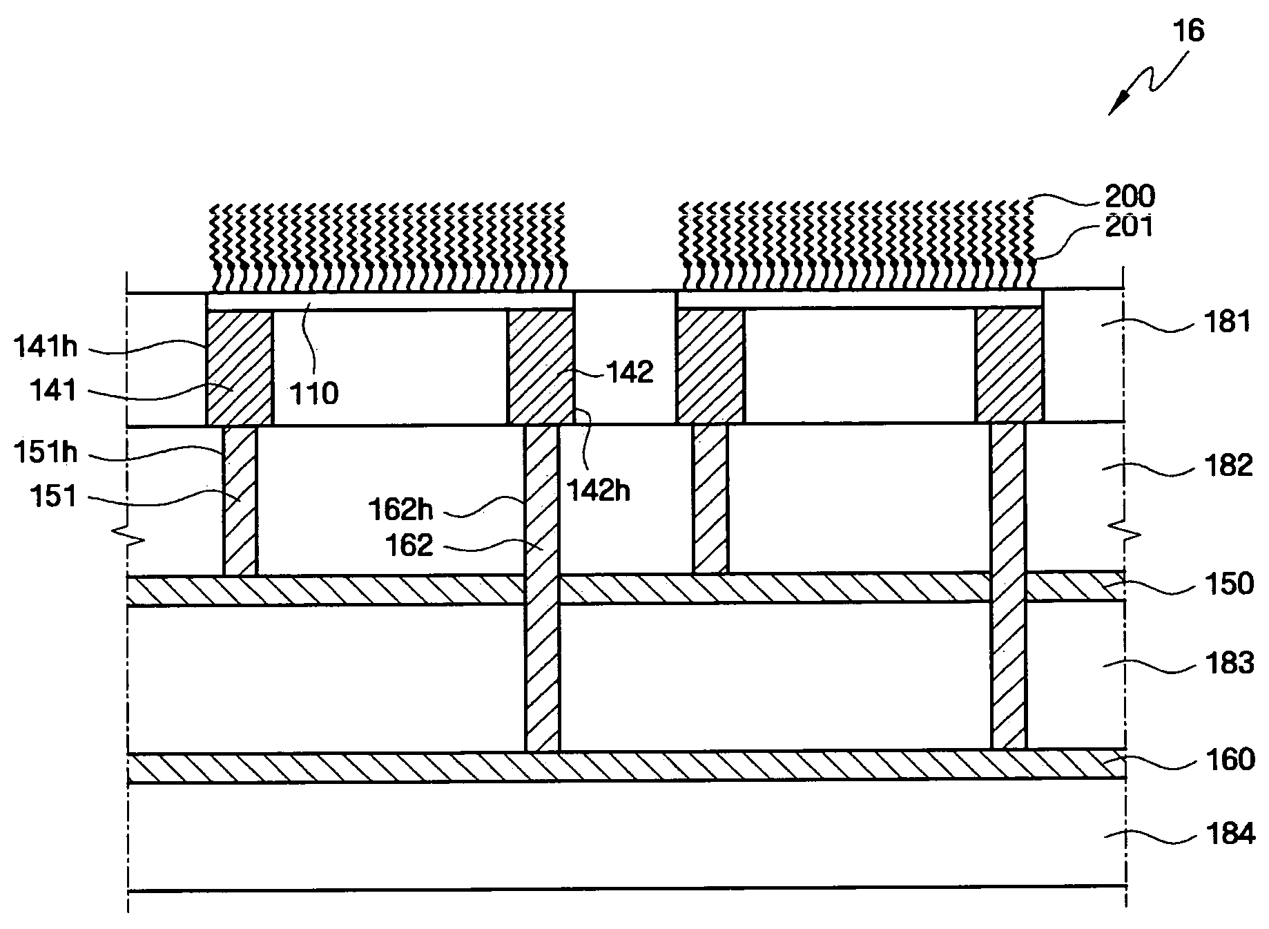
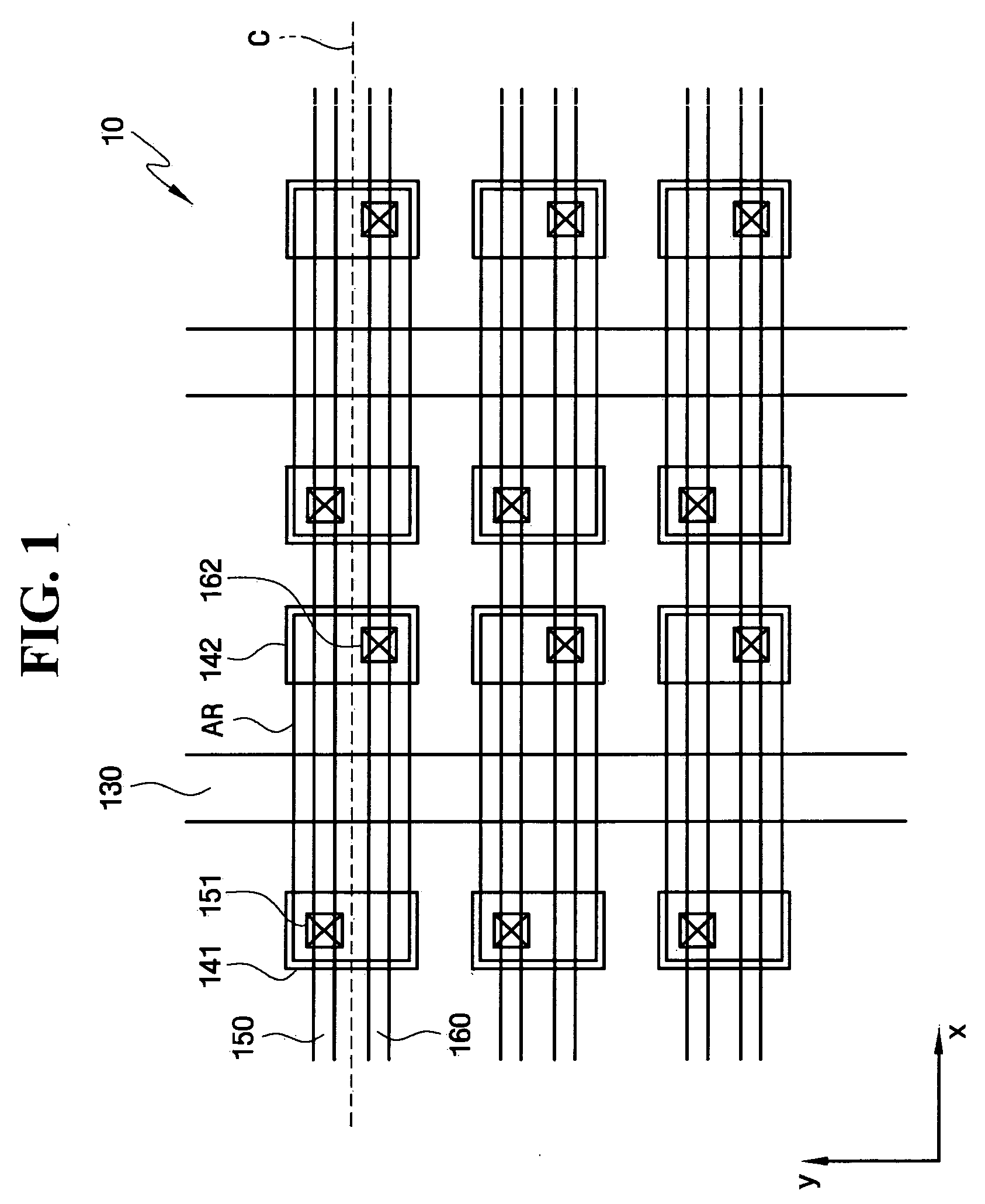
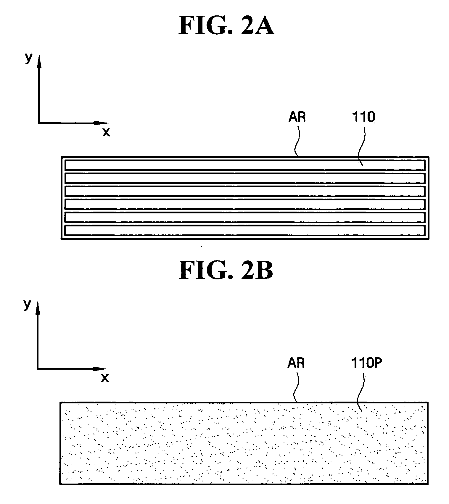
[0015]Advantages and features of example embodiments may be better appreciated upon review of the detailed description in conjunction with the accompanying drawings. However, it should be noted that example embodiments may be embodied in many different forms and should not be construed as being limited to the examples herein.

[0016]It will be understood that when an element or layer is referred to as being “on”, “connected to”, “coupled to”, or “covering” another element or layer, it may be directly on, connected to, coupled to, or covering the other element or layer or intervening elements or layers may be present. In contrast, when an element is referred to as being “directly on,”“directly connected to” or “directly coupled to” another element or layer, there are no intervening elements or layers present. Like numbers refer to like elements throughout the specification. As used herein, the term “and / or” includes any and all combinations of one or more of the associated listed items...


PUM


Abstract

Example embodiments relate to a biosensor using a nanoscale material as a channel of a transistor and a method of fabricating the same. A biosensor according to example embodiments may include a plurality of insulating films. A first signal line and a second signal line may be interposed between the plurality of insulating films. A semiconductor nanostructure may be disposed on the plurality of insulating films, the semiconductor nanostructure having a first side electrically connected to the first signal line and a second side electrically connected to the second signal line. A plurality of probes may be coupled to the semiconductor nanostructure. A biosensor according to example embodiments may have a reduced analysis time.

Description

PRIORITY STATEMENT[0001]The present application claims priority under 35 U.S.C. § 119 to Korean Patent Application No. 10-2007-0094290, filed on Sep. 17, 2007 in the Korean Intellectual Property Office (KIPO), the entire contents of which are incorporated herein by reference.BACKGROUND[0002]1. Technical Field[0003]Example embodiments of the present application relate to biosensors and methods of fabricating biosensors.[0004]2. Description of the Related Art[0005]Biosensors are used to analyze bio-samples by allowing the probes of a biosensor to interact with a bio-sample and observing which reactions occurred between the bio-sample and the probes. For instance, a fluorescent analysis may be used to analyze a bio-sample. In such an analysis, probes having different base sequences are fixed on corresponding cells of a biosensor by base sequence type, and a bio-sample marked with a fluorescent material is allowed to interact with the probes. Consequently, the fluorescent material may r...

Claims


Application Information

Patent Timeline
Patent Type & Authority Applications(United States)
IPC IPC(8): H01L21/28H01L29/772
CPCB82Y10/00B82Y15/00H01L51/0595G01N27/4145H01L2924/0002G01N27/4146H01L2924/00H10K10/701G01N27/414G01N33/48707G01N33/5308H01L23/485H01L23/5226H10K85/20H10K85/701G01N27/00B82B1/00B82B3/00
Inventor LEE, MOON-SOOKCHO, BYEONG-OKRYOO, MAN-HYOUNGYASUE, TAKAHIROHAH, JUNG-HWAN
Owner SAMSUNG ELECTRONICS CO LTD
Why Eureka
Try Eureka