Pixel structure of horizontal field liquid crystal display

a liquid crystal display and horizontal field technology, applied in non-linear optics, instruments, optics, etc., can solve the problems that the horizontal field lcd like an ips lcd and an ffs lcd cannot meet the requirements concerning the view angle, observer cannot see a normal image, and color deviation becomes so grea

Active Publication Date: 2009-04-02
BEIJING BOE OPTOELECTRONCIS TECH CO LTD +1
View PDF4 Cites 33 Cited by
  • Summary
  • Abstract
  • Description
  • Claims
  • Application Information

AI Technical Summary

Problems solved by technology

However, as the display panel of a LCD increases in size, a horizontal field LCD like an IPS LCD and an FFS LCD cannot any more meet the requirements concerning the view angle of a large size LCD, especially for the wide screen LCD over 40 inch.
Thus, when the view angle of an observer is not consistent with the view angle of the pixel structure, the observer cannot see a normal image.
In addition, when the view angle of the observer is approaching the limit of view angle of the display, the color deviation becomes so great that the visual effect of the observer is adversely affected.
That is, there is one or more pixels damaged in the display panel of the LCD during manufacture, and these pixels cannot function properly, which result in dark spots on the display panel and adversely influence the display quality of the LCD.

Method used


Image

  • Pixel structure of horizontal field liquid crystal display
  • Pixel structure of horizontal field liquid crystal display
  • Pixel structure of horizontal field liquid crystal display

Examples


first embodiment

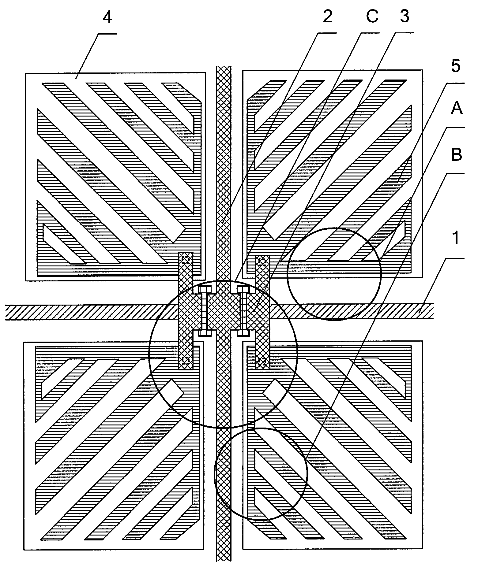
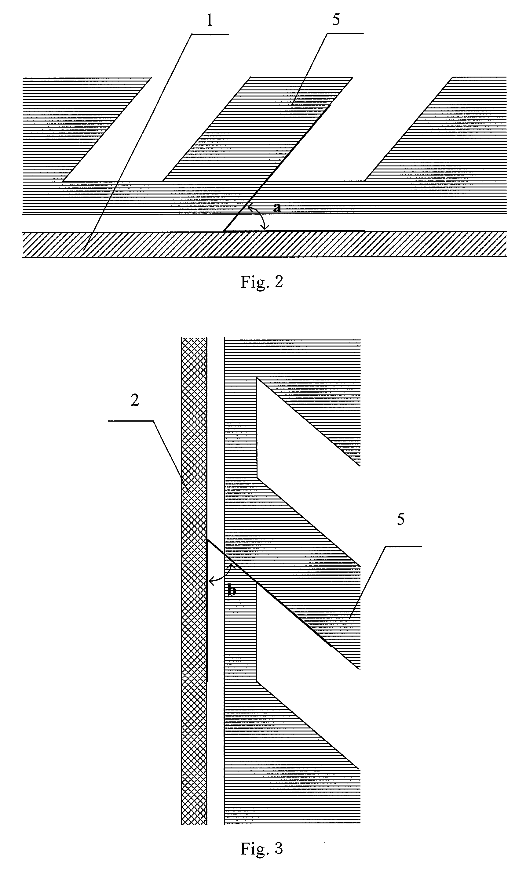
[0028]FIG. 1 is a structural diagram showing a pixel structure according to the first embodiment. As shown in FIG. 1, the pixel unit of the pixel structure comprises a gate line 1 corresponding to the pixel unit, a data line 2 corresponding to the pixel unit, two TFTs 3, four sub-pixels 4, and four pixel electrodes 5. The gate line 1 is arranged between the adjacent sub-pixels 4 of the pixel unit, the data line 2 is arranged between the adjacent sub-pixels 4 of the pixel unit, and the gate line 1 and data line 2 are perpendicular with each other. One of the TFTs 3 is electrically connected with the gate line 1, the data line 2, and two adjacent sub-pixels 4. One pixel electrode 5 is provided in each sub-pixel 4, and each of the pixel electrodes 5 is provided with a plurality of slits in a predetermined direction. Horizontal fields are created in the pixel unit for controlling the alignment of liquid crystal molecules.

[0029]In the pixel structure of the LCD according to this embodime...

second embodiment

[0039]FIG. 5 is a structural diagram showing a pixel structure according to the second embodiment. As shown in FIG. 5, the pixel unit comprises a gate line 1 corresponding to the pixel unit, a data line 2 corresponding to the pixel unit, four TFTs 3, four sub-pixels 4, and four pixel electrodes 5. The gate line 1 is arranged between the adjacent sub-pixels 4 in the pixel unit, the data line 2 is arranged between the adjacent sub-pixels 4 in the pixel unit, and the gate line 1 and data line 2 are perpendicular with each other. One of the TFTs 3 is electrically connected with the gate line 1, the data line 2, and one sub-pixel 4, i.e., each of the TFTs 3 corresponds to one of the sub-pixels 4. One pixel electrode 5 is provided in each sub-pixel 4, and each of the pixel electrodes 5 is provided with a plurality of slits in a predetermined direction. Horizontal fields are created in the pixel unit for controlling the alignment of liquid crystal molecules.

[0040]According to the pixel str...

third embodiment

[0041]FIG. 6 is a structural diagram showing a pixel structure according to the third embodiment. As shown in FIG. 6, the pixel unit comprises a gate line 1 corresponding to the pixel unit, a data line 2 corresponding to the pixel unit, two TFTs 3, four sub-pixels 4, and four pixel electrodes 5. The gate line 1 is arranged between the adjacent sub-pixels 4 in the pixel unit, the data line 2 is arranged between the adjacent sub-pixels 4 in the pixel unit, and the gate line 1 and data line 2 are perpendicular with each other. One of the TFTs 3 is electrically connected with the gate line 1, the data line 2, and two adjacent sub-pixels 4. One pixel electrode 5 is provided in each sub-pixel 4. Each of the pixel electrodes 5 is provided with a plurality of slits in a predetermined direction, and the slits in adjacent pixel electrodes 5 form a right angle. The slits of two pixel electrodes 5 are parallel with the gate line 1, and the other two pixel electrodes 5 are parallel with the data...


PUM

PropertyMeasurementUnit
sizeaaaaaaaaaa
angleaaaaaaaaaa
angleaaaaaaaaaa

Abstract

A pixel structure for a horizontal field LCD comprises a plurality of pixel units. Each of the pixel units comprises a gate line corresponding to the pixel unit, a data line corresponding to the pixel unit, and at least one TFT, wherein the TFT is electrically connected with the gate line and the data line, the gate line and the data line divide the pixel unit into four sub-pixels, the sub-pixel is provided with a pixel electrode which is electrically connected with the TFT, and the pixel electrode is provided with a plurality of slits in a predetermined direction.

Description

BACKGROUND OF THE INVENTION[0001]The present invention relates to a pixel structure of a liquid crystal display (LCD).[0002]An in-plane field switching (IPS) display rotates liquid crystal molecules by creating in-plane horizontal fields, and the horizontal fields are parallel with each other to improve the view angle performance of the LCD. The fringe field switching (FFS) display creates a fringe field between the electrodes, in which liquid crystal molecules between the electrodes and above the electrodes are rotated in plane for switching, so that the view angle performance of the LCD can be improved. However, as the display panel of a LCD increases in size, a horizontal field LCD like an IPS LCD and an FFS LCD cannot any more meet the requirements concerning the view angle of a large size LCD, especially for the wide screen LCD over 40 inch.[0003]In both the IPS LCD and FFS LCD, the pixel structure in the display panel forms the view angle in a same direction. Thus, when the vi...

Claims


Application Information

Patent Timeline
Patent Type & Authority Applications(United States)
IPC IPC(8): G02F1/1343
CPCG02F1/134363G02F2001/134372G02F2001/134345G02F1/134345G02F1/134372G02F1/1343
Inventor KIM, JAIKWANG
Owner BEIJING BOE OPTOELECTRONCIS TECH CO LTD
Why Eureka
Try Eureka