

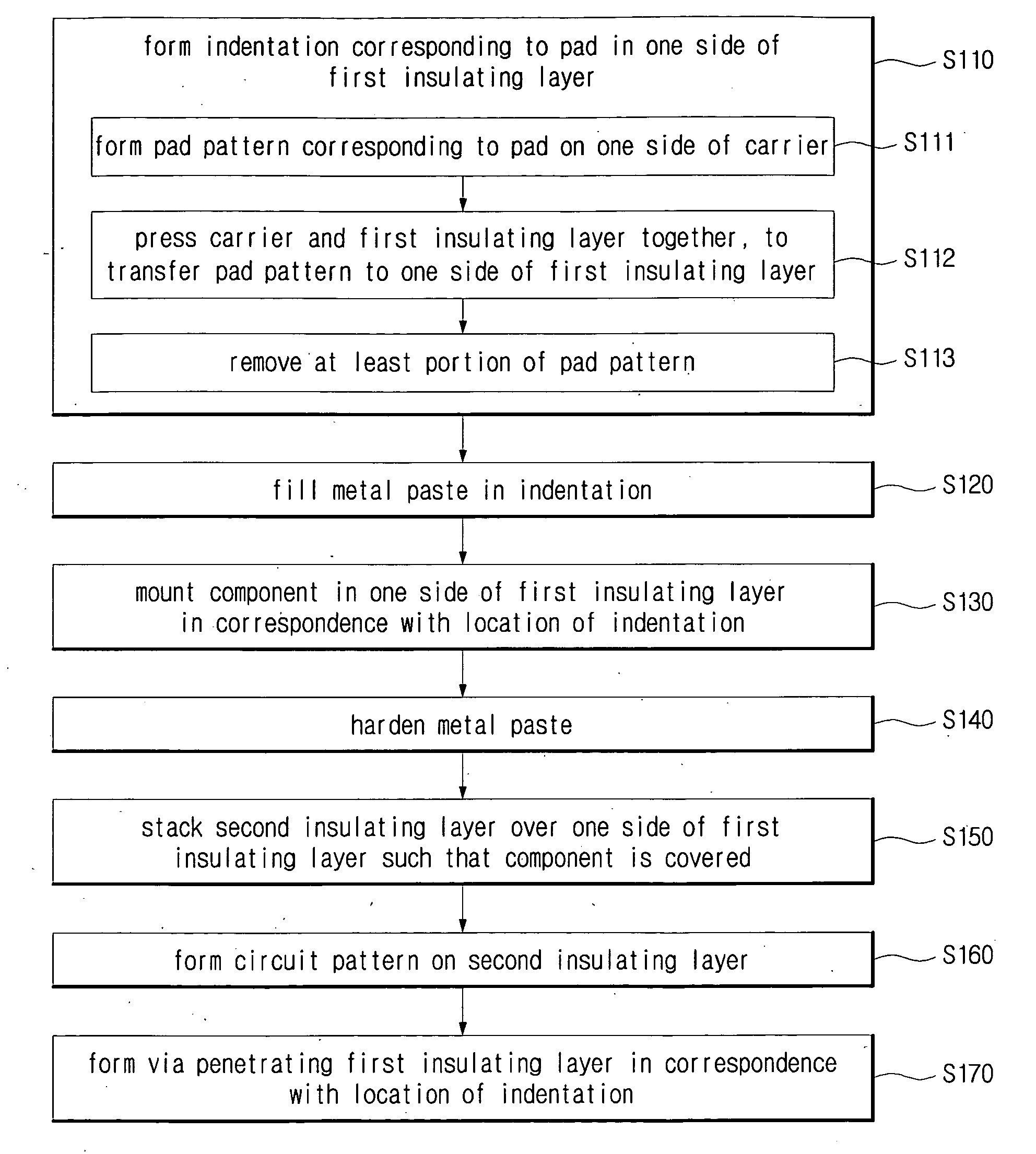
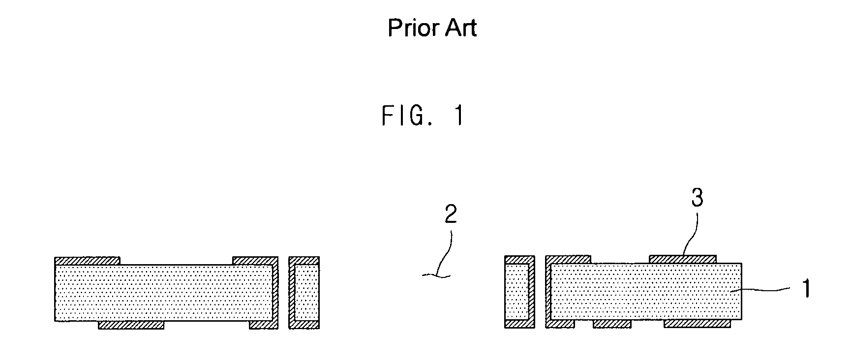
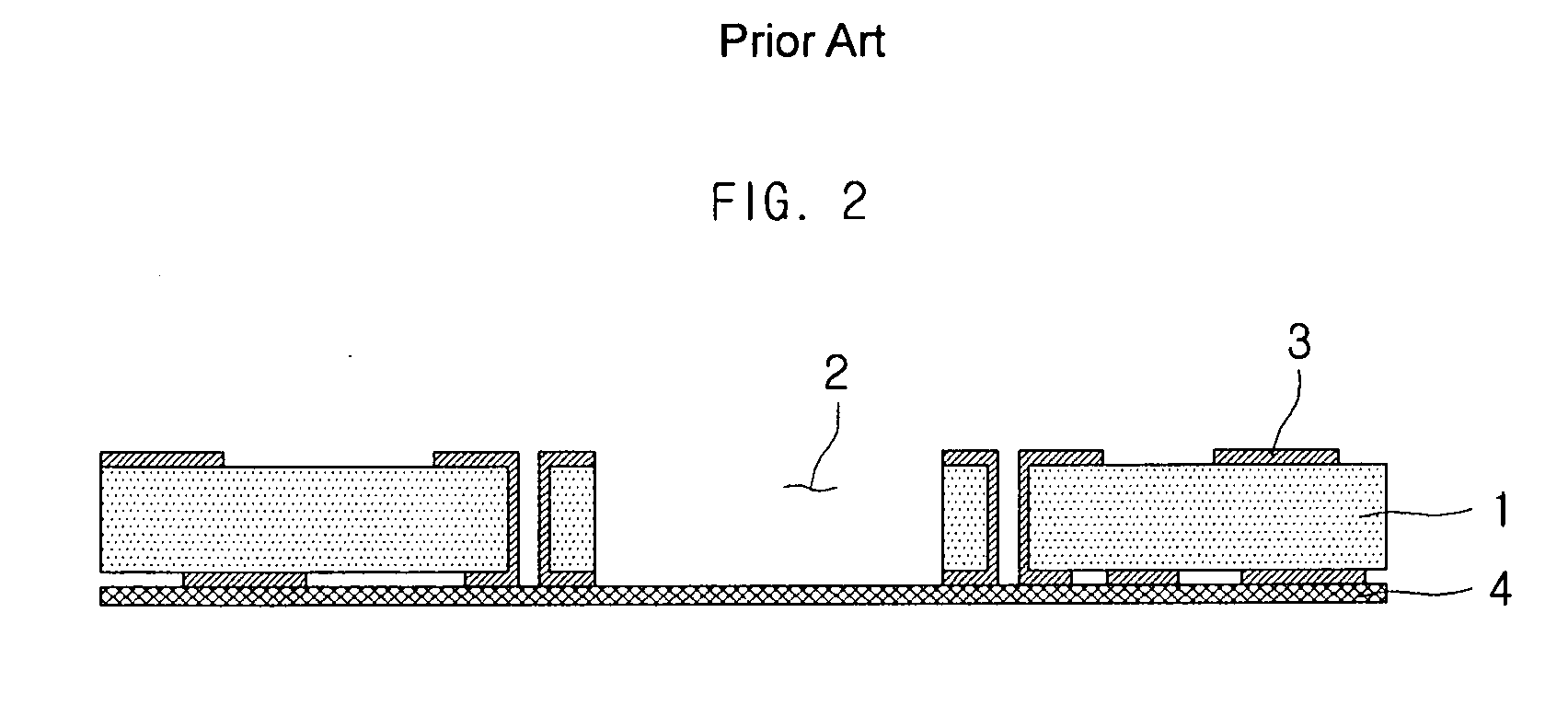
Method of manufacturing a package board
a technology of package boards and manufacturing methods, applied in the manufacture of printed circuits, printed circuit aspects, basic electric elements, etc., can solve the problems of reducing the overall reducing the thickness of the package board, so as to prevent damage to the component
- Summary
- Abstract
- Description
- Claims
- Application Information
AI Technical Summary
Benefits of technology
Problems solved by technology
Method used
Image

Examples
Embodiment Construction
[0023]As the invention allows for various changes and numerous embodiments, particular embodiments will be illustrated in the drawings and described in detail in the written description. However, this is not intended to limit the present invention to particular modes of practice, and it is to be appreciated that all changes, equivalents, and substitutes that do not depart from the spirit and technical scope of the present invention are encompassed in the present invention. In the description of the present invention, certain detailed explanations of related art are omitted when it is deemed that they may unnecessarily obscure the essence of the invention.
[0024]While such terms as “first,”“second,” etc., may be used to describe various elements, such elements must not be limited to the above terms. The above terms are used only to distinguish one element from another.
[0025]The terms used in the present specification are merely used to describe particular embodiments, and are not inte...
PUM
 Abstract
Description
Claims
Application Information